Introduction to HDI PCBs
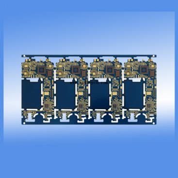
High-Density Interconnect (HDI) Printed Circuit Boards (PCBs) are advanced circuit boards that offer superior performance and functionality compared to traditional PCBs. HDI PCBs are characterized by their high component density, fine line widths, and small via sizes, enabling the creation of compact, lightweight, and highly efficient electronic devices. As technology continues to evolve, the demand for HDI PCBs has grown significantly across various industries, including consumer electronics, telecommunications, automotive, aerospace, and medical devices.
What are HDI PCBs?
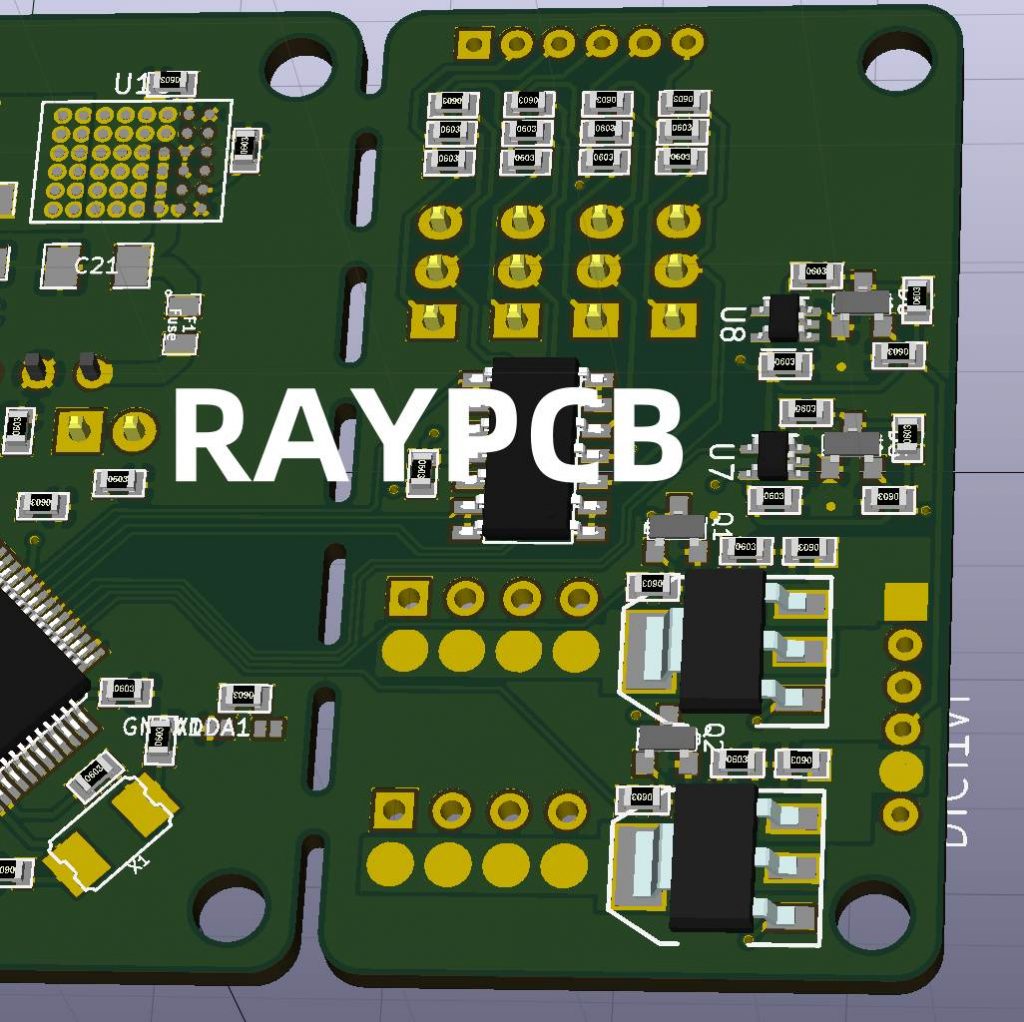
HDI PCBs are a type of printed circuit board that incorporates advanced manufacturing techniques to achieve higher component density and improved signal integrity. These boards feature finer trace widths, smaller via diameters, and thinner dielectric materials compared to conventional PCBs. HDI technology allows for the routing of traces between closely spaced vias and components, enabling the creation of highly complex designs within a compact form factor.
Advantages of HDI PCBs
- Miniaturization: HDI PCBs enable the miniaturization of electronic devices by allowing for higher component density and reduced board size.
- Improved Signal Integrity: The shorter trace lengths and reduced layer count in HDI PCBs minimize signal interference and improve overall signal integrity.
- Enhanced Reliability: HDI PCBs offer improved reliability due to the reduced number of interconnections and the use of advanced manufacturing techniques.
- Cost-Effective: Despite the initial higher cost, HDI PCBs can be cost-effective in the long run due to reduced assembly time, improved yield, and lower overall system cost.
- Flexibility in Design: HDI technology allows for greater design flexibility, enabling the creation of complex, high-performance electronic devices.
HDI PCB Manufacturing Techniques
Microvias
Microvias are small, laser-drilled holes that connect the outer layers of an HDI PCB to the inner layers. These vias have a diameter of less than 150 microns and are filled with conductive material, such as copper, to establish electrical connections between layers. Microvias enable higher routing density and improved signal integrity by reducing the distance signals need to travel.
Types of Microvias
- Blind Vias: Blind vias are drilled from the surface of the PCB and terminate at an inner layer, without penetrating through the entire board thickness.
- Buried Vias: Buried vias are located within the inner layers of the PCB and do not extend to either surface of the board.
- Stacked Vias: Stacked vias are formed by aligning microvias on top of each other across multiple layers, creating a continuous electrical connection.
Sequential Lamination
Sequential lamination is a process used in the manufacturing of HDI PCBs, where individual layers are laminated together in a specific sequence. This technique allows for the creation of complex, multi-layer boards with a high degree of precision and reliability. Sequential lamination enables the incorporation of microvias and fine-pitch components, resulting in higher-density designs.
Advanced Materials
HDI PCBs utilize advanced materials to achieve their superior performance characteristics. These materials include:
- High-Tg Laminates: High-glass transition temperature (Tg) laminates offer improved thermal stability and mechanical strength, ensuring the reliability of HDI PCBs under demanding conditions.
- Low-Loss Dielectrics: Low-loss dielectric materials minimize signal attenuation and distortion, enabling faster signal transmission and improved signal integrity.
- Thin Copper Foils: Thin copper foils, typically in the range of 12-18 microns, allow for finer trace widths and reduced layer thickness, contributing to the overall miniaturization of HDI PCBs.

HDI PCB Design Considerations
Design Rules
When designing HDI PCBs, engineers must adhere to specific design rules to ensure manufacturability, reliability, and optimal performance. These design rules include:
- Minimum Trace Width and Spacing: HDI PCBs require finer trace widths and spacing compared to traditional PCBs, typically in the range of 3-4 mils (75-100 microns).
- Via Size and Spacing: Microvias in HDI PCBs have smaller diameters and require tighter spacing rules compared to conventional through-hole vias.
- Pad Size and Pitch: HDI PCBs accommodate smaller component pad sizes and finer pitch, enabling higher component density.
- Copper Thickness: Thinner copper layers are used in HDI PCBs to achieve finer trace widths and reduced overall board thickness.
Signal Integrity
Ensuring signal integrity is crucial in HDI PCB design. To minimize signal distortion and interference, designers must consider the following factors:
- Impedance Control: Maintaining consistent impedance throughout the signal path is essential to prevent reflections and signal degradation.
- Crosstalk Reduction: Proper trace routing, shielding, and the use of ground planes can help minimize crosstalk between adjacent signals.
- Electromagnetic Interference (EMI) Mitigation: Appropriate shielding, grounding, and filtering techniques should be employed to reduce EMI and ensure compliance with regulatory standards.
Thermal Management
HDI PCBs often have higher power densities due to the increased component density, making thermal management a critical consideration. Designers must implement effective thermal management strategies to dissipate heat and prevent component failure. These strategies include:
- Thermal Vias: Thermal vias are used to transfer heat from high-power components to the PCB’s outer layers or dedicated heat sinks.
- Copper Pours: Copper pours on the outer layers of the PCB help distribute heat evenly and improve overall thermal conductivity.
- Thermal Interface Materials: Thermal interface materials, such as thermal pads or compounds, are used to enhance heat transfer between components and the PCB or heat sinks.

Applications of HDI PCBs
Consumer Electronics
HDI PCBs are widely used in consumer electronics, such as smartphones, tablets, wearables, and IoT devices. The miniaturization and high-performance capabilities of HDI technology enable the creation of sleek, feature-rich devices that meet consumer demands.
Telecommunications
In the telecommunications industry, HDI PCBs are employed in network equipment, 5G infrastructure, and fiber-optic systems. HDI technology enables the development of high-speed, high-bandwidth communication systems that can handle the ever-increasing data traffic.
Automotive Electronics
HDI PCBs are increasingly used in automotive electronics, particularly in advanced driver assistance systems (ADAS), infotainment systems, and electric vehicle powertrains. The robust and reliable nature of HDI PCBs makes them suitable for the harsh operating conditions encountered in automotive environments.
Aerospace and Defense
The aerospace and defense sectors rely on HDI PCBs for various applications, including avionics, radar systems, and satellite communications. HDI technology offers the high performance, reliability, and miniaturization required for these critical systems.
Medical Devices
HDI PCBs are utilized in medical devices, such as implantable devices, diagnostic equipment, and wearable health monitors. The compact size and high reliability of HDI PCBs make them suitable for the stringent requirements of the medical industry.
Future Trends in HDI PCBs
Advanced Manufacturing Processes
As the demand for HDI PCBs continues to grow, manufacturers are investing in advanced manufacturing processes to improve production efficiency and reduce costs. Some of these processes include:
- Laser Direct Imaging (LDI): LDI technology enables the direct transfer of circuit patterns onto the PCB, eliminating the need for traditional photomasks and improving registration accuracy.
- Additive Manufacturing: Additive manufacturing techniques, such as 3D printing, are being explored for the creation of HDI PCBs, offering greater design freedom and faster prototyping.
Emerging Materials
Researchers are continuously developing new materials to enhance the performance and reliability of HDI PCBs. Some emerging materials include:
- Graphene: Graphene, a two-dimensional carbon material, offers exceptional electrical and thermal conductivity, making it a promising candidate for future HDI PCBs.
- Ceramic Substrates: Ceramic substrates, such as aluminum nitride and silicon carbide, provide excellent thermal dissipation and mechanical stability, making them suitable for high-power HDI applications.
Integration with Advanced Packaging Technologies
HDI PCBs are increasingly being integrated with advanced packaging technologies, such as:
- System-in-Package (SiP): SiP technology combines multiple integrated circuits and passive components within a single package, utilizing HDI PCBs as the interconnect substrate.
- Wafer-Level Packaging (WLP): WLP involves the packaging of individual die at the wafer level, with HDI PCBs serving as the redistribution layer for the packaged devices.
Conclusion
High-Density Interconnect (HDI) Printed Circuit Boards have revolutionized the electronics industry by enabling the creation of compact, high-performance devices. With their superior signal integrity, enhanced reliability, and miniaturization capabilities, HDI PCBs have become essential in various sectors, including consumer electronics, telecommunications, automotive, aerospace, and medical devices.
As technology continues to advance, the demand for HDI PCBs is expected to grow, driven by the need for faster, smaller, and more efficient electronic systems. Manufacturers and designers must stay abreast of the latest advancements in HDI technology, including advanced manufacturing processes, emerging materials, and integration with cutting-edge packaging techniques.
By embracing HDI PCBs and their associated technologies, companies can develop innovative, high-performance products that meet the evolving needs of consumers and industries alike. As we move towards a more connected and technologically advanced future, HDI PCBs will undoubtedly play a crucial role in shaping the electronics landscape.
Frequently Asked Questions (FAQ)
- What is the difference between HDI PCBs and traditional PCBs?
HDI PCBs feature higher component density, finer trace widths, and smaller via sizes compared to traditional PCBs. These characteristics enable HDI PCBs to offer superior performance, miniaturization, and improved signal integrity. - What are the main applications of HDI PCBs?
HDI PCBs are widely used in various industries, including consumer electronics (smartphones, tablets, wearables), telecommunications (5G infrastructure, network equipment), automotive electronics (ADAS, infotainment systems), aerospace and defense (avionics, radar systems), and medical devices (implantable devices, diagnostic equipment). - What are the advantages of using microvias in HDI PCBs?
Microvias in HDI PCBs enable higher routing density and improved signal integrity by reducing the distance signals need to travel. They allow for the creation of complex, multi-layer designs within a compact form factor, contributing to the overall miniaturization of electronic devices. - What are the key design considerations for HDI PCBs?
When designing HDI PCBs, engineers must adhere to specific design rules, such as minimum trace width and spacing, via size and spacing, pad size and pitch, and copper thickness. Signal integrity and thermal management are also critical considerations, requiring the implementation of appropriate strategies to ensure optimal performance and reliability. - What are the future trends in HDI PCB technology?
Future trends in HDI PCB technology include the adoption of advanced manufacturing processes (e.g., Laser Direct Imaging, additive manufacturing), the development of emerging materials (e.g., graphene, ceramic substrates), and the integration with advanced packaging technologies (e.g., System-in-Package, Wafer-Level Packaging). These advancements aim to further enhance the performance, reliability, and cost-effectiveness of HDI PCBs.
| Characteristic | HDI PCBs | Traditional PCBs |
|---|---|---|
| Component Density | High | Low to Moderate |
| Trace Width | Fine (3-4 mils) | Wider (>4 mils) |
| Via Size | Small (<150 microns) | Larger (>150 microns) |
| Layer Count | High (8 or more) | Low to Moderate (1-6) |
| Signal Integrity | Superior | Good |
| Miniaturization | Excellent | Limited |
| Cost | Higher | Lower |
No responses yet