
Introduction to PCBs
Printed Circuit Boards (PCBs) are the backbone of modern electronics. They are used in almost every electronic device we use today, from smartphones and laptops to medical equipment and aerospace systems. PCBs are essential because they provide a platform for electronic components to be mounted and connected, allowing for the creation of complex circuits in a compact and efficient manner.
Types of PCBs
There are several types of PCBs, each with its own unique characteristics and applications. The most common types of PCBs include:
- Single-sided PCBs
- Double-sided PCBs
- Multi-layer PCBs
- Flexible PCBs
- Rigid-Flex PCBs
- High Density Interconnect (HDI) PCBs
What are HDI PCBs?
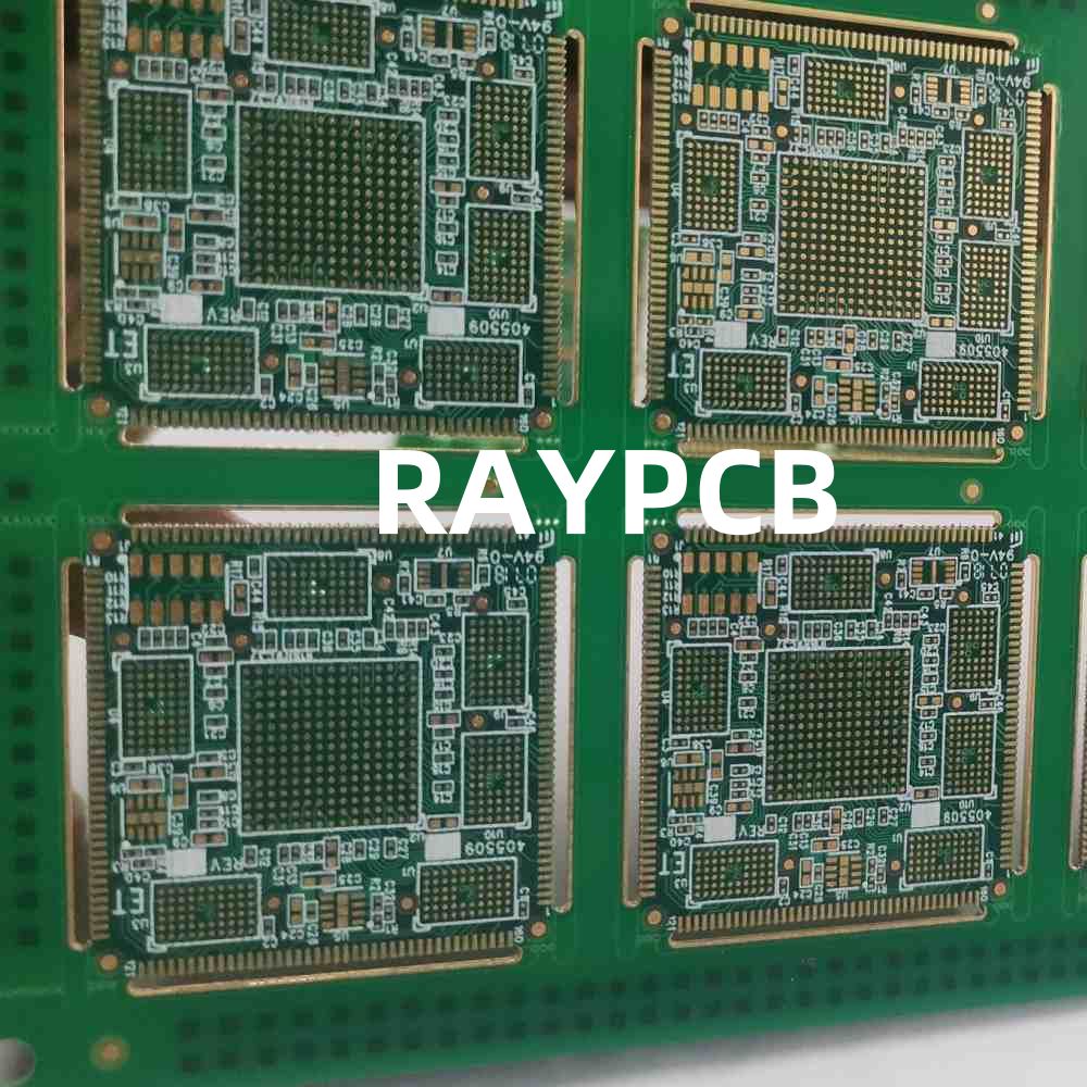
HDI PCBs are a type of printed circuit board that features a higher wiring density than traditional PCBs. They are designed to accommodate more components and interconnections in a smaller space, making them ideal for applications that require high performance, reliability, and miniaturization.
Characteristics of HDI PCBs
HDI PCBs have several unique characteristics that set them apart from other types of PCBs:
- High Density Interconnect: HDI PCBs have a higher wiring density than traditional PCBs, allowing for more interconnections in a smaller space.
- Smaller Via Sizes: HDI PCBs use smaller vias (holes that connect different layers of the PCB) than traditional PCBs, which allows for more efficient use of space and improved signal integrity.
- Thinner Traces: HDI PCBs have thinner traces (the copper pathways that carry electrical signals) than traditional PCBs, which allows for more precise control over signal routing and improved signal integrity.
- Blind and Buried Vias: HDI PCBs can incorporate blind and buried vias, which are vias that do not go through the entire thickness of the board. This allows for more efficient use of space and improved signal integrity.
Applications of HDI PCBs
HDI PCBs are used in a wide range of applications that require high performance, reliability, and miniaturization. Some of the most common applications of HDI PCBs include:
- Smartphones and Tablets: HDI PCBs are used in smartphones and tablets to accommodate the high density of components and interconnections required for these devices.
- Wearable Electronics: HDI PCBs are used in wearable electronics, such as smartwatches and fitness trackers, to provide high performance and reliability in a small form factor.
- Medical Devices: HDI PCBs are used in medical devices, such as pacemakers and implantable defibrillators, to provide high reliability and long-term performance in a compact package.
- Aerospace and Defense: HDI PCBs are used in aerospace and defense applications, such as satellites and military communications systems, to provide high performance and reliability in harsh environments.

Advantages of HDI PCBs
HDI PCBs offer several advantages over traditional PCBs, making them the perfect choice for many applications.
Miniaturization
One of the main advantages of HDI PCBs is their ability to accommodate more components and interconnections in a smaller space. This allows for the creation of smaller and more compact electronic devices, which is particularly important in applications where space is limited, such as smartphones and wearable electronics.
Improved Signal Integrity
HDI PCBs offer improved signal integrity compared to traditional PCBs. The smaller via sizes and thinner traces used in HDI PCBs allow for more precise control over signal routing, which reduces signal distortion and improves overall signal quality. This is particularly important in high-speed applications, such as 5G wireless communication systems.
Increased Reliability
HDI PCBs are designed to provide high reliability and long-term performance. The use of blind and buried vias, along with the improved signal integrity offered by HDI PCBs, helps to reduce the risk of signal degradation and failure over time. This is particularly important in applications where reliability is critical, such as medical devices and aerospace systems.
Cost Savings
While HDI PCBs may have a higher initial cost than traditional PCBs, they can offer significant cost savings over the long term. The ability to accommodate more components and interconnections in a smaller space can reduce the overall size and weight of electronic devices, which can lead to cost savings in materials and shipping. Additionally, the improved reliability and performance offered by HDI PCBs can reduce the need for repairs and replacements over time, further reducing overall costs.

Design Considerations for HDI PCBs
Designing HDI PCBs requires careful consideration of several factors to ensure optimal performance and reliability.
Layer Stackup
The layer stackup of an HDI PCB is critical to its performance and reliability. The number and arrangement of layers, along with the materials used for each layer, can have a significant impact on signal integrity and manufacturability. Designers must carefully consider the layer stackup to ensure that the PCB can accommodate the required components and interconnections while maintaining optimal performance.
Via Design
Via design is another critical consideration in HDI PCB design. The smaller via sizes used in HDI PCBs require careful placement and routing to ensure optimal signal integrity and manufacturability. Designers must also consider the use of blind and buried vias to further optimize space utilization and signal routing.
Signal Integrity Analysis
Signal integrity analysis is essential in HDI PCB design to ensure that the PCB can maintain optimal signal quality and reliability over time. Designers must carefully analyze the signal paths and impedances to ensure that the PCB can accommodate the required signal speeds and frequencies without degradation or interference.
Thermal Management
Thermal management is another important consideration in HDI PCB design. The high density of components and interconnections in HDI PCBs can generate significant amounts of heat, which can lead to performance degradation and failure over time. Designers must carefully consider the placement and routing of components and interconnections to ensure optimal thermal management and heat dissipation.
Manufacturing Process for HDI PCBs
The manufacturing process for HDI PCBs is more complex than traditional PCBs due to the higher density of components and interconnections.
Material Selection
The materials used in HDI PCBs must be carefully selected to ensure optimal performance and reliability. The substrate material, copper thickness, and laminate material must all be chosen based on the specific requirements of the application.
Drilling and Plating
The drilling and plating process for HDI PCBs is more precise than traditional PCBs due to the smaller via sizes and higher density of interconnections. The use of laser drilling and advanced plating techniques is often required to achieve the necessary precision and reliability.
Etching and Lamination
The etching and lamination process for HDI PCBs must be carefully controlled to ensure optimal signal integrity and reliability. The use of advanced etching and lamination techniques, such as sequential lamination and controlled depth drilling, is often required to achieve the necessary precision and performance.
Assembly and Testing
The assembly and testing process for HDI PCBs is more complex than traditional PCBs due to the higher density of components and interconnections. Advanced assembly techniques, such as flip-chip and chip-on-board, are often required to achieve the necessary precision and reliability. Thorough testing is also essential to ensure that the PCB meets the required performance and reliability standards.
FAQs
- What is the difference between HDI PCBs and traditional PCBs?
HDI PCBs have a higher density of components and interconnections than traditional PCBs, allowing for smaller and more compact electronic devices. They also offer improved signal integrity and reliability due to the use of smaller via sizes and thinner traces. - What are the main applications of HDI PCBs?
HDI PCBs are used in a wide range of applications that require high performance, reliability, and miniaturization, such as smartphones, wearable electronics, medical devices, and aerospace systems. - What are the advantages of using HDI PCBs?
The main advantages of HDI PCBs include miniaturization, improved signal integrity, increased reliability, and cost savings over the long term. - What are the key design considerations for HDI PCBs?
The key design considerations for HDI PCBs include layer stackup, via design, signal integrity analysis, and thermal management. - What are the main steps in the manufacturing process for HDI PCBs?
The main steps in the manufacturing process for HDI PCBs include material selection, drilling and plating, etching and lamination, and assembly and testing. Each step requires careful control and advanced techniques to achieve the necessary precision and reliability.
Conclusion
HDI PCBs are the perfect choice for applications that require high performance, reliability, and miniaturization. They offer several advantages over traditional PCBs, including improved signal integrity, increased reliability, and cost savings over the long term. However, designing and manufacturing HDI PCBs requires careful consideration of several factors, including layer stackup, via design, signal integrity analysis, and thermal management.
As electronic devices continue to become smaller and more complex, the demand for HDI PCBs is expected to grow. By understanding the characteristics, advantages, and design considerations of HDI PCBs, designers and manufacturers can create more advanced and reliable electronic devices that meet the needs of today’s demanding applications.
No responses yet