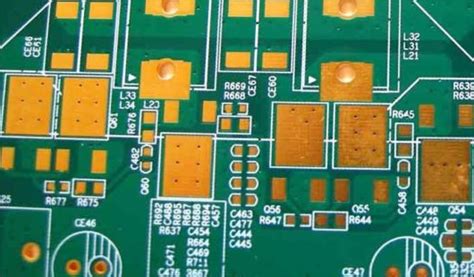
What is HDI PCB Design?
High Density Interconnect (HDI) PCB design is a printed circuit board design that incorporates higher wiring density per unit area to reduce the size and weight of the PCB. This is achieved through the use of smaller vias, finer pitch components, and thinner dielectric materials.
HDI PCB designs offer several advantages over traditional PCB designs:
- Smaller form factor and lighter weight
- Increased functionality within the same or smaller space
- Improved electrical performance
- Reduced power consumption
- Lower costs for high volume production
HDI PCB Design Guidelines
To create an optimal HDI PCB design, follow these key guidelines:
- Component Selection
- Use fine-pitch and small-outline components
- Consider using chip-scale packages (CSPs) and ball grid arrays (BGAs)
- Select components with compatible thermal characteristics
- Layer Stack-up
- Use a minimum of 4 layers, typically 8-12 layers for complex designs
- Incorporate thin dielectric materials to reduce overall thickness
- Follow manufacturer’s recommendations for stack-up configuration
- Via Types and Sizes
- Employ microvias and buried vias for higher density interconnects
- Adhere to manufacturer’s specifications for via sizes and spacing
- Use via-in-pad where necessary to maximize wiring density
- Routing and Spacing
- Route traces with appropriate width and spacing based on signal requirements
- Maintain symmetry and balance in differential pairs
- Avoid sharp angles and use curved traces for improved signal integrity
- Power and Ground Planes
- Provide adequate power and ground planes for power distribution and shielding
- Use appropriate plane capacitance and avoid large plane cuts
- Implement proper decoupling and bypassing techniques
- Signal Integrity and EMI
- Perform signal integrity simulations to ensure proper termination and impedance matching
- Follow best practices for high-speed design, such as length matching and avoiding stubs
- Implement EMI reduction techniques, such as shielding and proper grounding
HDI PCB Manufacturing Considerations
When designing HDI PCBs, it’s crucial to consider the manufacturing process and capabilities:
- Choose a reputable PCB manufacturer with experience in HDI fabrication
- Provide clear and detailed manufacturing files and specifications
- Communicate any special requirements or constraints early in the design process
- Consider the impact of HDI features on manufacturing costs and lead times
- Conduct thorough testing and inspection to ensure manufacturability and reliability
HDI PCB Layer Stack-up
The layer stack-up is a critical aspect of HDI PCB design, as it determines the overall thickness, electrical properties, and manufacturability of the board. A typical HDI PCB stack-up consists of multiple layers of copper foil, separated by thin dielectric materials.
Common HDI PCB Layer Stack-ups
| Layer Count | Layer Configuration | Typical Thickness |
|---|---|---|
| 4 | Signal-Ground-Power-Signal | 0.8 mm – 1.0 mm |
| 6 | Signal-Ground-Signal-Ground-Power-Signal | 1.0 mm – 1.2 mm |
| 8 | Signal-Ground-Signal-Ground-Power-Ground-Signal-Signal | 1.2 mm – 1.6 mm |
| 10 | Signal-Ground-Signal-Ground-Power-Ground-Signal-Ground-Signal-Signal | 1.6 mm – 2.0 mm |
When deciding on the layer stack-up, consider the following factors:
- Number of signals and power/ground planes required
- Impedance requirements for controlled impedance traces
- Dielectric material properties and thickness
- Via structure and routing requirements
- Manufacturing capabilities and constraints

HDI PCB Via Types and Structures
HDI PCB designs utilize various types of vias to achieve higher wiring density and interconnect between layers. The most common via types used in HDI PCBs are:
- Microvia: A small-diameter via, typically less than 150 µm, that connects the outer layers to the inner layers. Microvias can be stacked or staggered to create interconnections between multiple layers.
- Buried Via: A via that connects inner layers without reaching the outer layers. Buried vias are used to create interconnections between internal layers without consuming space on the outer layers.
- Blind Via: A via that connects an outer layer to an inner layer without reaching the opposite outer layer. Blind vias are used to create interconnections between the outer layers and internal layers.
- Through Via: A traditional via that connects all layers, from the top to the bottom of the PCB. Through vias are used for interconnections that span the entire thickness of the board.
HDI Via Structures
HDI PCB designs can employ various via structures to achieve the desired interconnections and wiring density. Some common via structures include:
- Stacked Vias: Multiple microvias stacked on top of each other to create interconnections between multiple layers.
- Staggered Vias: Microvias arranged in a staggered pattern to create interconnections between layers while avoiding the need for stacking.
- Via-in-Pad: A via placed directly within a component pad to maximize wiring density and minimize the PCB footprint.
- Skip Vias: A via that skips one or more layers to create an interconnection between non-adjacent layers.
When selecting via types and structures, consider the following factors:
- Required interconnections and wiring density
- Manufacturing capabilities and constraints
- Signal integrity and electrical performance requirements
- Reliability and thermal management considerations

HDI PCB Routing and Layout
Proper routing and layout techniques are essential for creating a successful HDI PCB design. Here are some key considerations and best practices:
Trace Width and Spacing
- Use appropriate trace widths based on the required current carrying capacity and impedance requirements.
- Maintain adequate spacing between traces to minimize crosstalk and signal integrity issues.
- Follow manufacturer’s guidelines for minimum trace width and spacing based on the PCB fabrication capabilities.
Differential Pair Routing
- Route differential pairs with controlled impedance and symmetry to maintain signal integrity.
- Keep differential pair traces closely coupled and of equal length to minimize skew and phase differences.
- Avoid splitting differential pairs or routing them through different layers whenever possible.
High-Speed Signal Routing
- Use appropriate routing techniques for high-speed signals, such as length matching and avoiding stubs.
- Implement proper termination and impedance matching to minimize reflections and signal distortion.
- Consider the use of serpentine routing or delay lines to match trace lengths and timing.
Component Placement and Fanout
- Place components strategically to minimize trace lengths and optimize signal paths.
- Use component fanout techniques, such as via-in-pad or dog-bone fanout, to route traces efficiently from high-density components.
- Consider the placement of power and ground pins to minimize loop inductance and improve power integrity.
Power and Ground Planes
- Provide sufficient power and ground planes for power distribution and shielding.
- Use appropriate plane capacitance and avoid large plane cuts to minimize impedance discontinuities.
- Implement proper decoupling and bypassing techniques to reduce power supply noise and ensure signal integrity.
By following these routing and layout best practices, designers can create HDI PCB layouts that are optimized for performance, reliability, and manufacturability.
HDI PCB Signal Integrity and EMI Considerations
Signal integrity (SI) and electromagnetic interference (EMI) are critical aspects of HDI PCB design that must be carefully considered to ensure proper operation and compliance with industry standards.
Signal Integrity
- Perform SI simulations to analyze signal quality, reflections, and crosstalk.
- Use appropriate termination techniques, such as series termination or differential termination, to minimize signal reflections and ensure proper impedance matching.
- Minimize the use of vias, especially for high-speed signals, to reduce discontinuities and reflections.
- Implement proper grounding and shielding techniques to minimize noise and crosstalk.
Electromagnetic Interference
- Follow best practices for EMI reduction, such as proper grounding, shielding, and filtering.
- Use appropriate layout techniques, such as ground planes and guard traces, to minimize radiated emissions.
- Consider the use of spread-spectrum clocking or other EMI reduction techniques for high-speed digital signals.
- Perform EMI simulations and testing to ensure compliance with relevant EMC standards, such as FCC Part 15 or EN 55022.
Power Integrity
- Provide adequate power and ground planes for power distribution and return paths.
- Use appropriate decoupling capacitors and power supply filtering to minimize power supply noise and ensure stable voltage levels.
- Minimize the inductance of power and ground connections to reduce voltage fluctuations and improve transient response.
- Perform power integrity simulations to analyze voltage drops, current density, and power supply noise.
By addressing signal integrity, EMI, and power integrity considerations throughout the HDI PCB design process, designers can ensure robust and reliable performance in the final product.
Frequently Asked Questions (FAQ)
- What is the minimum feature size for HDI PCB designs?
The minimum feature size for HDI PCB designs depends on the specific manufacturer and their fabrication capabilities. Typically, HDI PCBs can achieve trace widths and spacing down to 50-75 µm, and microvia diameters down to 75-100 µm. However, some advanced HDI PCB manufacturers can offer even finer feature sizes. - How does the cost of HDI PCBs compare to traditional PCBs?
HDI PCBs generally have higher manufacturing costs compared to traditional PCBs due to the additional complexity and precision required in the fabrication process. However, the cost difference can be offset by the reduced PCB size, improved performance, and higher functionality achieved with HDI designs. Additionally, for high-volume production, the cost per unit can be competitive with traditional PCBs. - What are the challenges in designing HDI PCBs?
Some of the challenges in designing HDI PCBs include: - Ensuring proper signal integrity and managing high-speed signals
- Achieving optimal component placement and routing density
- Minimizing electromagnetic interference (EMI) and ensuring EMC compliance
- Selecting appropriate materials and stack-up configurations
- Collaborating effectively with PCB manufacturers to ensure manufacturability and reliability
- Can HDI PCBs be used for high-power applications?
Yes, HDI PCBs can be used for high-power applications, but special considerations must be taken to ensure adequate power handling and thermal management. This includes using appropriate trace widths and copper weights for high-current paths, providing sufficient power and ground planes, and implementing proper thermal management techniques, such as thermal vias and heatsinks. - What are the testing and inspection requirements for HDI PCBs?
HDI PCBs require thorough testing and inspection to ensure proper functionality, reliability, and conformance to specifications. Some common testing and inspection methods include: - Automated Optical Inspection (AOI) for detecting surface defects and component placement issues
- X-ray inspection for evaluating internal structures, such as vias and solder joints
- Electrical testing, including continuity, isolation, and impedance testing
- Functional testing to verify the performance of the assembled PCB
- Environmental testing, such as thermal cycling and humidity exposure, to assess reliability under various conditions
By understanding the design guidelines, manufacturing considerations, and testing requirements, engineers can create HDI PCB designs that are optimized for performance, reliability, and cost-effectiveness.
No responses yet