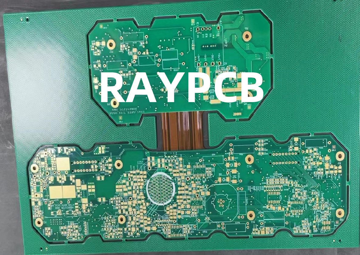
What are HDI PCBs?
HDI PCBs, or High Density Interconnect Printed Circuit Boards, are advanced circuit boards that feature a higher wiring density than traditional PCBs. This is achieved through the use of smaller vias, finer traces, and multiple layers. HDI PCBs allow for more components to be placed in a smaller area, resulting in compact and lightweight devices.
The main characteristics of HDI PCBs include:
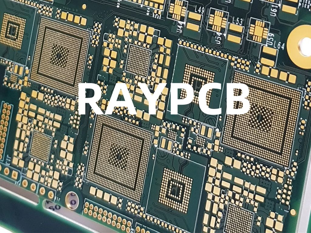
– Smaller vias (microvias) with diameters less than 150 microns
– Finer traces with widths less than 100 microns
– Higher layer counts (typically 8 or more)
– Blind and buried vias for increased connectivity
– Sequential lamination for building complex structures
Benefits of HDI PCBs
HDI PCBs offer numerous benefits over traditional PCBs, making them the preferred choice for many industries, including consumer electronics, automotive, aerospace, and medical devices. Some of the key benefits include:
1. Miniaturization
With the ability to pack more components into a smaller space, HDI PCBs enable the creation of compact and lightweight devices. This is particularly important for portable electronics, wearables, and IoT devices where size and weight are critical factors.
2. Enhanced Performance
The shorter signal paths and reduced parasitic capacitance in HDI PCBs result in improved signal integrity and faster signal transmission. This translates to better overall performance, higher frequencies, and lower power consumption.
3. Increased Reliability
HDI PCBs feature a higher level of interconnect reliability due to the use of microvias and advanced manufacturing processes. This reduces the risk of signal interruptions and improves the overall reliability of the end product.
4. Cost-Effective
Although HDI PCBs may have a higher initial cost compared to traditional PCBs, they offer long-term cost savings through reduced assembly time, fewer components, and improved yield rates. Additionally, the compact size of HDI PCBs allows for more boards to be produced per panel, further reducing manufacturing costs.

HDI PCB Manufacturing Process
The manufacturing process for HDI PCBs is more complex than that of traditional PCBs due to the higher density and smaller features. Here’s a general overview of the HDI PCB manufacturing process:
- Design and Stackup Planning: The PCB design is created using EDA software, and the layer stackup is planned based on the design requirements and HDI guidelines.
- Material Selection: High-quality, high-Tg materials are chosen for the PCB substrate to ensure reliability and performance.
- Drilling and Plating: Microvias are drilled using laser or mechanical drilling methods, and the holes are plated with copper to create electrical connections between layers.
- Patterning: The copper layers are patterned using photolithography and etching processes to create the desired circuit patterns.
- Lamination: The individual layers are laminated together using heat and pressure to form a solid board.
- Surface Finishing: A surface finish, such as ENIG (Electroless Nickel Immersion Gold) or HASL (Hot Air Solder Leveling), is applied to protect the exposed copper and improve solderability.
- Electrical Testing: The completed HDI PCB undergoes electrical testing to ensure proper functionality and adherence to specifications.

Choosing the Right HDI PCB Manufacturing Partner
Selecting the right HDI PCB manufacturing partner is crucial for the success of your project. Here are some key factors to consider when choosing a manufacturer:
1. Experience and Expertise
Look for a manufacturer with extensive experience in producing HDI PCBs and a proven track record of delivering high-quality boards. They should have a deep understanding of HDI design guidelines, material selection, and advanced manufacturing processes.
2. State-of-the-Art Facilities
Ensure that the manufacturer has invested in state-of-the-art equipment and facilities to handle the complex manufacturing processes required for HDI PCBs. This includes advanced laser drilling machines, high-precision patterning equipment, and automated testing systems.
3. Quality Control and Certifications
Choose a manufacturer that adheres to strict quality control standards and holds relevant certifications, such as ISO 9001, IATF 16949, and UL. These certifications demonstrate the manufacturer’s commitment to quality and reliability.
4. Communication and Support
Effective communication is key to a successful partnership. Look for a manufacturer that offers responsive support, clear communication channels, and a dedicated project management team to ensure smooth collaboration throughout the project lifecycle.
5. Scalability and Flexibility
As your business grows, your HDI PCB requirements may change. Choose a manufacturer that can scale production to meet your evolving needs and offer flexibility in terms of design changes, lead times, and order quantities.
HDI PCB Design Considerations
Designing HDI PCBs requires careful consideration of various factors to ensure optimal performance and manufacturability. Here are some key design considerations:
1. Layer Stackup
The layer stackup is a critical aspect of HDI PCB design. It determines the number of layers, the placement of microvias, and the overall thickness of the board. Work closely with your manufacturer to develop an optimal layer stackup that meets your design requirements and HDI guidelines.
2. Via Types and Placement
HDI PCBs utilize different types of vias, including blind, buried, and stacked vias. Careful placement of these vias is essential to ensure proper connectivity and signal integrity. Follow the manufacturer’s design rules and guidelines for via placement and spacing.
3. Trace Width and Spacing
To achieve higher density, HDI PCBs feature finer traces and tighter spacing compared to traditional PCBs. Ensure that your design adheres to the manufacturer’s minimum trace width and spacing requirements to avoid manufacturability issues and signal integrity problems.
4. Signal Integrity
High-speed signals in HDI PCBs are more susceptible to signal integrity issues, such as crosstalk and impedance mismatch. Use appropriate design techniques, such as proper grounding, shielding, and impedance matching, to mitigate these issues and ensure reliable signal transmission.
5. Thermal Management
With a higher component density, HDI PCBs generate more heat than traditional PCBs. Incorporate adequate thermal management techniques, such as the use of thermal vias, heatsinks, and proper component placement, to dissipate heat effectively and prevent thermal-related failures.
HDI PCB Testing and Inspection
To ensure the quality and reliability of HDI PCBs, rigorous testing and inspection processes are essential. Here are some common testing and inspection methods used for HDI PCBs:
1. Automated Optical Inspection (AOI)
AOI uses high-resolution cameras and advanced image processing algorithms to inspect the PCB for defects such as missing components, solder bridges, and incorrect component placement. This automated process allows for fast and accurate inspection of HDI PCBs.
2. X-Ray Inspection
X-ray inspection is used to examine the internal structure of HDI PCBs, including the microvias and multilayer interconnects. This non-destructive testing method helps identify defects such as voids, cracks, and delamination that may not be visible from the surface.
3. Electrical Testing
Electrical testing, such as flying probe testing and in-circuit testing (ICT), verifies the electrical connectivity and functionality of the HDI PCB. These tests ensure that the board meets the specified electrical performance requirements and identify any short circuits, open circuits, or component failures.
4. Microsectioning
Microsectioning involves cross-sectioning the HDI PCB and examining the internal structure under a microscope. This destructive testing method provides detailed information about the quality of the plating, the integrity of the microvias, and the lamination of the layers.
5. Thermal Cycling
Thermal cycling tests expose the HDI PCB to repeated cycles of extreme temperature changes to assess its ability to withstand thermal stresses. This test helps identify potential reliability issues related to thermal expansion mismatches and delamination.
Industry Applications of HDI PCBs
HDI PCBs find applications in a wide range of industries due to their superior performance, compact size, and reliability. Some of the key industries that rely on HDI PCBs include:
1. Consumer Electronics
HDI PCBs are extensively used in consumer electronics, such as smartphones, tablets, laptops, and wearables. The compact size and high-density interconnects of HDI PCBs enable the creation of sleek and feature-rich devices that meet consumer demands.
2. Automotive Electronics
The automotive industry increasingly relies on HDI PCBs for advanced driver assistance systems (ADAS), infotainment systems, and electrification components. HDI PCBs provide the necessary reliability and performance required for safety-critical automotive applications.
3. Aerospace and Defense
HDI PCBs are used in aerospace and defense applications, such as avionics systems, radar equipment, and satellite communication devices. The high-density interconnects and robust construction of HDI PCBs ensure reliable operation in harsh environments and extreme conditions.
4. Medical Devices
Medical devices, such as implantable devices, diagnostic equipment, and wearable health monitors, utilize HDI PCBs for their compact size, high reliability, and advanced functionality. HDI PCBs enable the development of miniaturized medical devices that improve patient care and outcomes.
5. Industrial Automation
HDI PCBs are used in industrial automation systems, such as robotics, machine vision, and process control equipment. The high-speed signal transmission and dense interconnects of HDI PCBs enable the development of advanced industrial automation solutions that enhance productivity and efficiency.
The Future of HDI PCBs
As technology continues to advance and the demand for smaller, faster, and more powerful devices grows, HDI PCBs will play an increasingly critical role in shaping the future of electronics. Some of the emerging trends and developments in HDI PCBs include:
1. Higher Density Interconnects
The push for miniaturization will drive the development of even higher density interconnects in HDI PCBs. This will involve the use of smaller microvias, finer traces, and advanced materials to enable the creation of ultra-compact devices with enhanced functionality.
2. Advanced Materials
New materials, such as low-loss dielectrics, high-temperature substrates, and embedded components, will be incorporated into HDI PCBs to improve performance, reliability, and thermal management. These advanced materials will enable HDI PCBs to meet the demanding requirements of emerging applications, such as 5G, IoT, and artificial intelligence.
3. 3D Packaging
3D packaging technologies, such as package-on-package (PoP) and system-in-package (SiP), will increasingly rely on HDI PCBs as the interconnect backbone. HDI PCBs will enable the vertical stacking of multiple components and packages, allowing for even greater miniaturization and functional integration.
4. Intelligent PCBs
The integration of sensors, antennas, and other smart components directly into HDI PCBs will give rise to intelligent PCBs. These PCBs will have the ability to sense, process, and communicate data, enabling new applications in wearables, IoT, and smart systems.
5. Sustainable Manufacturing
As environmental concerns grow, there will be a greater emphasis on sustainable manufacturing practices for HDI PCBs. This will involve the use of eco-friendly materials, green manufacturing processes, and responsible waste management to minimize the environmental impact of PCB production.
Frequently Asked Questions (FAQ)
1. What is the difference between HDI PCBs and traditional PCBs?
HDI PCBs feature higher wiring density, smaller vias, finer traces, and more layers compared to traditional PCBs. This allows for greater miniaturization, improved performance, and increased reliability.
2. What are the main applications of HDI PCBs?
HDI PCBs are widely used in consumer electronics, automotive electronics, aerospace and defense, medical devices, and industrial automation. They are particularly suitable for applications that require compact size, high performance, and reliability.
3. What are the challenges in designing HDI PCBs?
Designing HDI PCBs requires careful consideration of factors such as layer stackup, via types and placement, trace width and spacing, signal integrity, and thermal management. Designers must adhere to strict design rules and guidelines to ensure manufacturability and optimal performance.
4. How do I choose the right HDI PCB manufacturing partner?
When choosing an HDI PCB manufacturing partner, consider factors such as experience and expertise, state-of-the-art facilities, quality control and certifications, communication and support, and scalability and flexibility. Look for a manufacturer that can meet your specific requirements and provide reliable, high-quality HDI PCBs.
5. What is the future outlook for HDI PCBs?
The future of HDI PCBs is promising, with ongoing developments in higher density interconnects, advanced materials, 3D packaging, intelligent PCBs, and sustainable manufacturing. As technology advances and the demand for smaller, faster, and more powerful devices grows, HDI PCBs will continue to play a crucial role in shaping the electronics industry.
Conclusion
HDI PCBs have revolutionized the electronics industry, enabling the creation of compact, high-performance devices that meet the ever-increasing demands of modern applications. By understanding the benefits, manufacturing processes, design considerations, and industry applications of HDI PCBs, businesses can leverage this technology to develop innovative products and stay ahead of the competition.
Choosing the right HDI PCB manufacturing partner is essential for the success of your project. Look for a manufacturer with the experience, expertise, and state-of-the-art facilities to deliver high-quality HDI PCBs that meet your specific requirements. With the right partner and a commitment to innovation, you can unlock the full potential of HDI PCBs and drive the future of electronics.
No responses yet