Introduction to PCB Solutions and Tips
Printed Circuit Boards (PCBs) are essential components in modern electronics. They provide a way to mechanically support and electrically connect electronic components using conductive pathways, tracks or signal traces etched from copper sheets laminated onto a non-conductive substrate.
Designing and manufacturing PCBs can be a complex process with many factors to consider. This guide provides useful tips and best practices to help optimize your PCB solutions and avoid common pitfalls. By following these PCB Tips, you can improve the reliability, performance, and manufacturability of your PCB designs.
Key Considerations for PCB Design
When designing a PCB, there are several key factors to keep in mind:
1. Board Size and Shape
The size and shape of your PCB will be determined by the space constraints of your enclosure and the placement of components. Consider the following tips:
- Keep the board as small as possible to minimize cost and improve reliability
- Use standard board sizes when possible to avoid custom tooling charges
- Leave adequate space around the edges of the board for mounting holes and connectors
- Consider using irregular board shapes to fit into tight spaces
2. Layer Stack-up
The number of layers in your PCB Stack-up will depend on the complexity of your design and the required functionality. Here are some tips for optimizing your layer stack-up:
- Use the minimum number of layers required to route all signals
- Place signal layers adjacent to ground or power planes to minimize crosstalk
- Use thicker copper for power and ground layers to improve current carrying capacity
- Consider using blind and buried vias to minimize board size and improve routing density
| Layer | Typical Thickness (mils) | Material | Function |
|---|---|---|---|
| Top | 1.4 | Copper | Signal routing, component placement |
| Ground | 0.7 | Copper | Ground plane |
| Signal 1 | 0.7 | Copper | Signal routing |
| Power | 0.7 | Copper | Power plane |
| Signal 2 | 0.7 | Copper | Signal routing |
| Bottom | 1.4 | Copper | Signal routing, component placement |
3. Component Placement
Proper component placement is critical for manufacturability, reliability, and performance. Follow these tips:
- Group related components together to minimize trace lengths and improve signal integrity
- Place components on both sides of the board to maximize available space
- Avoid placing components too close to the edge of the board to prevent damage during manufacturing
- Consider the mounting orientation of components to minimize assembly errors
4. Routing and Trace Width
The routing of traces on your PCB can have a significant impact on signal integrity and EMI. Here are some tips for optimizing your routing:
- Use the shortest possible trace lengths to minimize signal reflections and attenuation
- Avoid sharp corners and use 45-degree angles instead to minimize signal reflections
- Use appropriate trace widths for the current carrying requirements of each signal
- Maintain consistent trace impedances to minimize signal reflections
| Signal Type | Typical Trace Width (mils) |
|---|---|
| Power | 20-100 |
| Ground | 20-100 |
| High-speed signals | 5-10 |
| Low-speed signals | 10-20 |
5. Via Design
Vias are used to connect traces on different layers of the PCB. Proper via design is important for signal integrity and manufacturability. Consider these tips:
- Use the smallest possible via size to minimize board space and improve routing density
- Avoid placing vias under components to prevent solder wicking and tombstoning
- Use thermal relief connections for vias connected to large copper areas to prevent solder wicking
- Consider using microvias for high-density designs
6. Solder Mask and Silkscreen
The solder mask and silkscreen layers provide insulation and labeling for your PCB. Here are some tips for optimizing these layers:
- Use a high-contrast color for the silkscreen to improve readability
- Avoid placing silkscreen over pads or vias to prevent adhesion problems
- Leave adequate clearance around pads and vias for the solder mask to prevent solder bridging
- Consider using a matte finish for the solder mask to improve the adhesion of conformal coatings
7. Design for Manufacturing (DFM)
Designing your PCB with manufacturing in mind can help reduce costs and improve yields. Follow these DFM tips:
- Use standard component sizes and packages when possible to minimize custom tooling costs
- Avoid using components with fine pitch or BGA packages unless absolutely necessary
- Provide adequate clearance around components for pick-and-place machines and soldering equipment
- Use consistent pad sizes and shapes to minimize the number of stencils required for solder paste application

PCB Manufacturing Process
Once your PCB design is complete, it will need to be manufactured. The manufacturing process typically involves the following steps:
- PCB Fabrication
- Solder Paste Application
- Component Placement
- Soldering
- Inspection and Testing
Here are some tips for optimizing the manufacturing process:
- Choose a reputable PCB manufacturer with experience in your type of design
- Provide clear and complete documentation, including Gerber files, bill of materials, and assembly drawings
- Communicate any special requirements or constraints to the manufacturer upfront
- Allow adequate time for fabrication and assembly to avoid rushing the process
- Perform thorough testing and inspection to ensure the quality of the finished product

Common PCB Design Mistakes to Avoid
Despite best efforts, mistakes can happen in PCB design. Here are some common mistakes to avoid:
- Incorrect component footprints
- Insufficient clearance between components
- Incorrect layer stack-up
- Inadequate power and ground connections
- Failing to consider manufacturability
- Inadequate or incorrect labeling
- Forgetting to include test points
- Not performing a design review
- Rushing the design process
- Not prototyping before full production
By being aware of these common mistakes and taking steps to avoid them, you can improve the quality and reliability of your PCB designs.

Advanced PCB Design Techniques
For more complex or high-performance PCB designs, there are several advanced techniques that can be employed:
High-Speed Design
High-speed digital signals require special consideration in PCB design to maintain signal integrity and minimize EMI. Some tips for high-speed design include:
- Use controlled impedance traces to match the impedance of the source and load
- Minimize trace lengths and use termination resistors to reduce reflections
- Use differential signaling for high-speed data transfer
- Provide adequate ground planes and use ground stitching vias to minimize ground bounce
RF Design
PCBs for radio frequency (RF) applications require special design techniques to minimize signal loss and interference. Some tips for RF PCB design include:
- Use high-frequency laminate materials with low dielectric loss
- Minimize trace lengths and use mitered corners to reduce signal reflections
- Use ground planes and shields to minimize interference
- Provide adequate grounding for components and use multiple vias for low-impedance connections
Flex PCBs
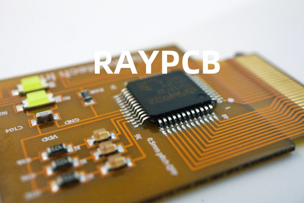
Flexible PCBs offer unique advantages in certain applications, such as wearable electronics or tight spaces. Some tips for flex PCB design include:
- Use flexible substrates with the appropriate bend radius and fatigue life
- Minimize the number of layers to reduce stiffness and improve flexibility
- Use strain relief features such as slots or cutouts to reduce stress on components
- Consider the mechanical and environmental stresses the flex PCB will be subjected to
High-Density Interconnect (HDI)
HDI PCBs use microvias and fine-pitch components to achieve very high routing density. Some tips for HDI PCB Design include:
- Use microvias and buried vias to minimize layer count and improve routing density
- Use high-resolution imaging and precision alignment to achieve fine features
- Consider using stacked or staggered microvias to further increase routing density
- Use high-quality materials and processes to ensure reliability and yield
PCB Testing and Inspection
Thorough testing and inspection are critical to ensure the quality and reliability of your PCBs. Here are some common testing and inspection methods:
Visual Inspection
Visual inspection is the first step in PCB testing and can catch many common defects such as solder bridging, component misalignment, or damaged traces. Automated optical inspection (AOI) machines can perform high-speed, high-resolution inspections.
X-Ray Inspection
X-ray inspection can reveal defects that are not visible on the surface, such as voids in solder joints or misaligned BGA components. X-ray inspection is particularly useful for high-density designs with hidden connections.
In-Circuit Testing (ICT)
ICT uses a bed-of-nails fixture to make electrical contact with test points on the PCB and verify the continuity and functionality of each component and connection. ICT can catch opens, shorts, and incorrect component values.
Functional Testing
Functional testing verifies that the PCB performs its intended function under real-world operating conditions. This may include testing for signal integrity, power consumption, or environmental stresses such as temperature or vibration.
Boundary Scan Testing
Boundary scan testing uses a special test access port (TAP) to test the interconnections between components on the PCB. This can be useful for identifying opens, shorts, or other defects in hard-to-reach areas of the board.
Frequently Asked Questions (FAQ)
1. What is the difference between a single-sided and double-sided PCB?
A single-sided PCB has components and traces on only one side of the board, while a double-sided PCB has components and traces on both sides. Double-sided PCBs offer more routing flexibility and higher component density, but are more complex and expensive to manufacture.
2. What is the purpose of a ground plane in a PCB?
A ground plane is a large area of copper that is connected to the ground potential of the circuit. It serves several purposes, including providing a low-impedance return path for signals, minimizing ground bounce and EMI, and providing shielding between layers.
3. What is the difference between through-hole and surface-mount components?
Through-hole components have leads that are inserted into holes drilled in the PCB and soldered on the opposite side, while surface-mount components are soldered directly onto pads on the surface of the board. Surface-mount components are smaller and allow for higher component density, but require more precise manufacturing processes.
4. What is the purpose of a soldermask layer on a PCB?
The soldermask layer is a thin insulating layer that covers the copper traces on the PCB, leaving only the pads and other exposed areas uncovered. It serves to protect the traces from oxidation and prevent solder bridging between adjacent pads or traces.
5. What is the difference between a prototype and a production PCB?
A prototype PCB is a small batch of boards used for testing and validation before mass production, while a production PCB is the final version of the board used in the end product. Prototypes may have looser tolerances and use different materials or processes than production boards to reduce cost and lead time.
Conclusion
Designing and manufacturing high-quality PCBs requires careful consideration of many factors, from component selection and placement to routing and testing. By following the tips and best practices outlined in this guide, you can optimize your PCB designs for reliability, performance, and manufacturability.
Remember to consider the key factors such as board size and shape, layer stack-up, component placement, routing, via design, soldermask and silkscreen, and design for manufacturing. Use advanced techniques such as high-speed design, RF design, flex PCBs, and HDI when appropriate for your application.
Finally, don’t neglect the importance of thorough testing and inspection to ensure the quality and reliability of your finished product. By catching defects early and verifying functionality, you can avoid costly rework and field failures.
With these PCB tips and techniques in mind, you can create PCB solutions that meet your specific needs and exceed your expectations. Happy designing!

No responses yet