What are PCBs?
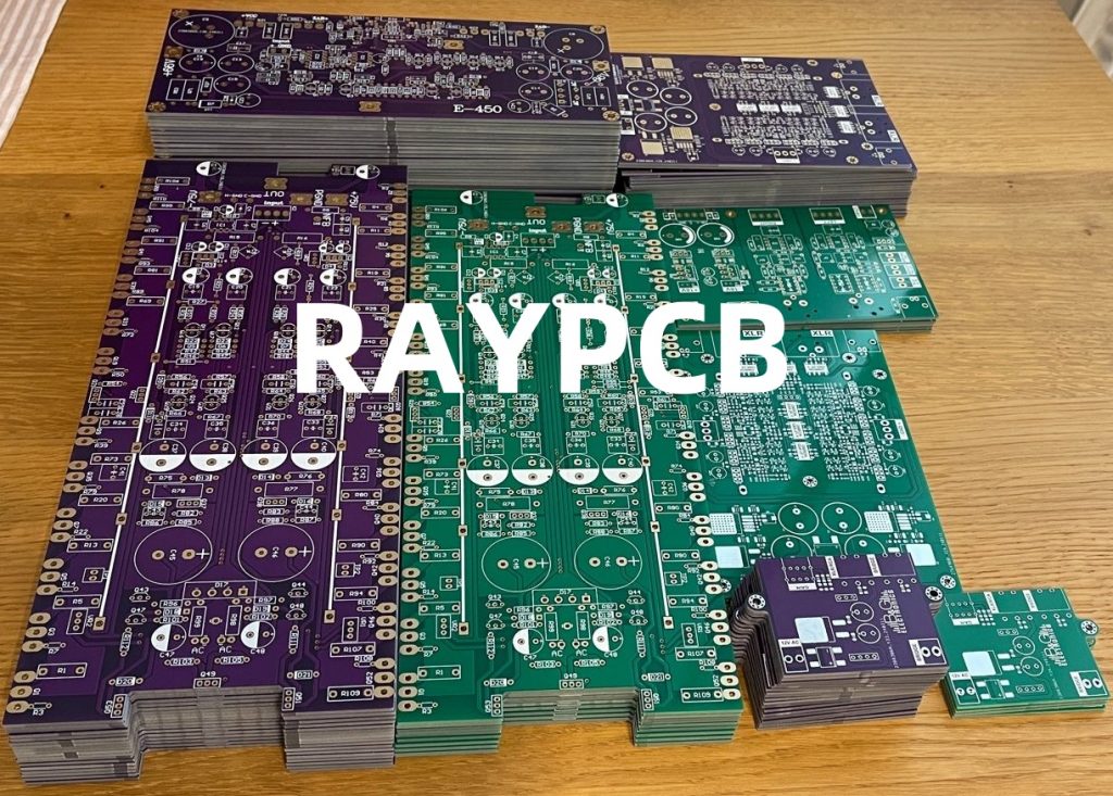
PCBs are flat boards made of insulating materials, such as fiberglass or plastic, with conductive pathways etched onto them. These pathways, known as traces, connect various electronic components, such as resistors, capacitors, and integrated circuits (ICs), to form a complete electronic circuit. PCBs can be single-sided, double-sided, or multi-layered, depending on the complexity of the circuit and the space constraints of the device.
Types of PCBs
There are several types of PCBs, each with its own unique characteristics and applications:
- Single-sided PCBs: These PCBs have conductive traces on only one side of the board. They are the simplest and most cost-effective type of PCB, suitable for low-complexity circuits.
- Double-sided PCBs: These PCBs have conductive traces on both sides of the board, allowing for more complex circuits and higher component density. The two sides are connected using vias, which are small holes drilled through the board and plated with conductive material.
- Multi-layer PCBs: These PCBs have multiple layers of conductive traces, separated by insulating layers. They offer the highest level of complexity and density, making them ideal for advanced electronic devices, such as smartphones and computer motherboards.
- Flexible PCBs: These PCBs are made of flexible materials, such as polyimide, allowing them to bend and fold without damaging the conductive traces. They are commonly used in wearable electronics and medical devices.
- Rigid-Flex PCBs: These PCBs combine the benefits of rigid and flexible PCBs, with rigid sections for mounting components and flexible sections for connecting them. They are often used in aerospace and military applications, where high reliability and durability are critical.
PCB Design Process
The PCB design process involves several steps, from concept to final production. Here’s a brief overview of the main stages:
- Schematic design: The first step is to create a schematic diagram of the electronic circuit, showing all the components and their connections. This is usually done using electronic design automation (EDA) software, such as Altium Designer or KiCad.
- Component selection: Once the schematic is complete, the next step is to select the appropriate components for the circuit. This involves considering factors such as power requirements, operating conditions, and cost.
- PCB layout: With the schematic and components finalized, the PCB layout can be designed. This involves placing the components on the board and routing the conductive traces between them. The layout must follow various design rules, such as minimum trace width and spacing, to ensure proper functionality and manufacturability.
- Design verification: Before sending the PCB design for manufacturing, it must be thoroughly checked for errors and potential issues. This includes running design rule checks (DRCs) and performing simulations to verify the circuit’s performance.
- Prototyping: Once the design is verified, a prototype PCB can be manufactured to test the actual circuit. This allows for any necessary modifications to be made before mass production.
PCB Manufacturing Process
The PCB manufacturing process involves several steps, each requiring specialized equipment and expertise. Here’s a detailed look at the main stages:
1. PCB Fabrication
The first stage of PCB manufacturing is the fabrication of the bare board. This involves the following steps:
- Material selection: The appropriate substrate material is selected based on the PCB’s requirements, such as thermal stability, dielectric constant, and mechanical strength. Common materials include FR-4, polyimide, and ceramic.
- Copper cladding: A thin layer of copper foil is bonded to the substrate material using heat and pressure. The copper layer will form the conductive traces of the PCB.
- Drilling: Holes are drilled through the board to accommodate through-hole components and vias. The drilling process can be done mechanically or using laser drilling for smaller, more precise holes.
- Plating: The drilled holes are plated with copper to create conductive pathways between the layers of the PCB. This is typically done using electroless copper plating, followed by electrolytic copper plating for increased thickness.
- Patterning: The desired circuit pattern is transferred onto the copper layer using a photolithographic process. This involves applying a light-sensitive resist to the copper, exposing it to UV light through a photomask, and developing the resist to reveal the desired pattern.
- Etching: The exposed copper is etched away using a chemical solution, leaving only the desired conductive traces. The remaining resist is then stripped away, revealing the final copper pattern.
- Soldermask application: A layer of soldermask is applied to the board to protect the copper traces and prevent accidental short circuits. The soldermask is typically green, but other colors are available for specific applications.
- Silkscreen printing: A silkscreen layer is printed onto the board to add text, logos, and component identifiers. This helps with assembly and troubleshooting.
- Surface finish: A surface finish, such as HASL (Hot Air Solder Leveling), ENIG (Electroless Nickel Immersion Gold), or OSP (Organic Solderability Preservative), is applied to the exposed copper to prevent oxidation and enhance solderability.
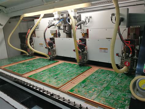
2. PCB Assembly
Once the bare board is fabricated, the electronic components can be mounted onto it. This process is known as PCB assembly, and it can be done using several methods:
- Through-hole assembly: Components with long leads are inserted through the holes in the board and soldered onto the opposite side. This method is suitable for larger components and provides strong mechanical connections.
- Surface mount assembly: Components with small, flat leads are mounted directly onto the surface of the board and soldered in place. This method allows for higher component density and faster assembly times.
- Mixed assembly: A combination of through-hole and surface mount components can be used on the same board, depending on the specific requirements of the circuit.
The PCB assembly process typically involves the following steps:
- Solder paste application: A thin layer of solder paste is applied to the pads on the board using a stencil or screen printing process. The solder paste consists of tiny solder spheres suspended in a flux matrix.
- Component placement: The components are placed onto the board using automated pick-and-place machines or by hand for smaller batches. The components are precisely aligned with the pads on the board.
- Reflow soldering: The board is passed through a reflow oven, which heats the solder paste to its melting point, allowing it to flow and form a strong bond between the components and the board.
- Inspection: The assembled board is visually inspected for any defects, such as misaligned components, solder bridges, or insufficient solder joints. Automated optical inspection (AOI) systems can be used for faster and more accurate inspections.
- Testing: The assembled board is tested to ensure proper functionality and performance. This can include in-circuit testing (ICT), functional testing, and boundary scan testing, depending on the complexity of the circuit and the required level of reliability.

Advanced PCB Manufacturing Techniques
As electronic devices become more complex and compact, advanced PCB manufacturing techniques have been developed to meet the increasing demands for higher density, better performance, and improved reliability. Some of these techniques include:
- HDI (High Density Interconnect) PCBs: HDI PCBs feature finer traces, smaller vias, and higher layer counts than traditional PCBs. This allows for higher component density and improved signal integrity, making them ideal for advanced applications, such as 5G phones and IoT devices.
- Embedded components: Instead of mounting components on the surface of the board, they can be embedded within the layers of the PCB. This saves space and improves performance by reducing the distance between components and minimizing signal delays.
- 3D printing: Additive manufacturing techniques, such as 3D printing, can be used to create PCBs with complex geometries and unique features. This enables the creation of custom-shaped boards and the integration of non-electronic elements, such as sensors and antennas.
- Flex-rigid PCBs: Combining the benefits of flexible and rigid PCBs, flex-rigid boards offer the flexibility to conform to unique shapes while providing the stability and durability of rigid sections. This makes them suitable for applications with limited space or demanding mechanical requirements.
- Advanced materials: New substrate materials, such as high-frequency laminates and thermally conductive materials, are being developed to improve the performance and reliability of PCBs in challenging environments, such as high-speed communications and power electronics.
Quality Control and Standards
To ensure the quality and reliability of PCBs, manufacturers must adhere to various industry standards and implement strict quality control measures throughout the production process. Some of the key standards and practices include:
- IPC standards: The Association Connecting Electronics Industries (IPC) develops and maintains a set of standards for PCB design, fabrication, and assembly. These standards, such as IPC-A-600 (Acceptability of Printed Boards), IPC-6012 (Qualification and Performance Specification for Rigid Printed Boards), and IPC-J-STD-001 (Requirements for Soldered Electrical and Electronic Assemblies), provide guidelines for ensuring the quality and reliability of PCBs.
- ISO standards: The International Organization for Standardization (ISO) develops and maintains standards for various industries, including electronics manufacturing. ISO 9001 (Quality Management Systems) and ISO 14001 (Environmental Management Systems) are commonly adopted by PCB manufacturers to demonstrate their commitment to quality and environmental responsibility.
- Testing and inspection: PCB manufacturers employ various testing and inspection methods to ensure the quality of their products. These include automated optical inspection (AOI), X-ray inspection, in-circuit testing (ICT), and functional testing. By catching defects early in the production process, manufacturers can minimize waste and improve overall quality.
- Traceability: Maintaining traceability throughout the PCB manufacturing process is crucial for identifying and addressing quality issues. This involves tracking materials, processes, and equipment used in each step of production, as well as maintaining detailed records of testing and inspection results.
Environmental Considerations
As with any manufacturing process, PCB production has an impact on the environment. To minimize this impact and promote sustainability, PCB manufacturers are adopting various eco-friendly practices and materials:
- Lead-free assembly: Traditional solder contains lead, which is a toxic substance that can harm human health and the environment. Many PCB manufacturers have transitioned to lead-free solder alloys, such as tin-silver-copper (SAC), to comply with regulations and reduce their environmental footprint.
- Halogen-free materials: Some PCB materials, such as FR-4, contain halogens (bromine and chlorine) that can release toxic fumes when burned. Halogen-free materials, such as polyphenylene ether (PPE) and polyethylene naphthalate (PEN), offer a safer and more environmentally friendly alternative.
- Recycling and waste management: PCB manufacturers are implementing recycling programs to recover valuable materials, such as copper and precious metals, from waste PCBs. They are also adopting better waste management practices to minimize the release of hazardous substances into the environment.
- Energy efficiency: By investing in energy-efficient equipment and optimizing their production processes, PCB manufacturers can reduce their energy consumption and minimize their carbon footprint.
Future Trends in PCB Manufacturing
As technology continues to advance, PCB manufacturing must evolve to keep pace with the changing demands of the electronics industry. Some of the key trends shaping the future of PCB manufacturing include:
- Miniaturization: The trend towards smaller, more compact electronic devices is driving the need for ever-smaller PCBs with higher component density. This requires advanced manufacturing techniques, such as HDI and embedded components, to achieve the necessary form factors and performance.
- 5G and IoT: The rollout of 5G networks and the growth of the Internet of Things (IoT) are creating new opportunities and challenges for PCB manufacturers. These applications require high-frequency, low-loss materials and advanced manufacturing techniques to ensure reliable performance in demanding environments.
- Automotive and aerospace: As vehicles and aircraft become more reliant on electronic systems, the demand for high-reliability PCBs is growing. PCB manufacturers are developing new materials and processes to meet the stringent requirements of these industries, such as high-temperature operation and resistance to vibration and shock.
- Sustainable manufacturing: With increasing global awareness of environmental issues, PCB manufacturers are under pressure to adopt more sustainable practices. This includes using eco-friendly materials, reducing waste and energy consumption, and implementing closed-loop recycling systems.
- Industry 4.0: The integration of advanced technologies, such as artificial intelligence, machine learning, and the Industrial Internet of Things (IIoT), is transforming PCB manufacturing. These technologies enable greater automation, real-time monitoring, and predictive maintenance, leading to improved efficiency, quality, and flexibility in PCB production.
Frequently Asked Questions (FAQs)
- What is the difference between a PCB and a PCBA?
A PCB (Printed Circuit Board) is the bare board with copper traces and pads, without any components mounted on it. A PCBA (Printed Circuit Board Assembly) is a PCB with electronic components soldered onto it, forming a complete functional circuit. - How long does it take to manufacture a PCB?
The lead time for PCB manufacturing depends on various factors, such as the complexity of the design, the number of layers, and the quantity ordered. For simple, low-volume orders, the lead time can be as short as 24 hours. For more complex, high-volume orders, the lead time can range from several days to several weeks. - What is the minimum feature size achievable in PCB manufacturing?
The minimum feature size depends on the manufacturing capabilities of the PCB fabricator. For standard PCBs, the minimum trace width and spacing is typically around 0.006 inches (0.15 mm). For HDI PCBs, the minimum feature size can be as small as 0.002 inches (0.05 mm) or less. - What is the difference between a prototype PCB and a production PCB?
A prototype PCB is a small batch of boards manufactured to test and validate the design before mass production. Prototype PCBs may have looser tolerances and may be fabricated using different processes than production PCBs. A production PCB is a large batch of boards manufactured to the final specifications and tolerances, using the optimized processes for high-volume production. - How can I ensure the quality and reliability of my PCBs?
To ensure the quality and reliability of your PCBs, it is important to work with a reputable PCB manufacturer that adheres to industry standards and implements strict quality control measures. This includes using high-quality materials, following best practices for design and manufacturing, and conducting thorough testing and inspection throughout the production process. It is also important to communicate your specific requirements and expectations to your manufacturer and to maintain open lines of communication throughout the project.
Conclusion
PCB manufacturing is a complex and constantly evolving field that plays a crucial role in the development of modern electronic devices. From the basics of PCB design and fabrication to the advanced techniques and materials used in cutting-edge applications, there is a wealth of knowledge and expertise required to produce high-quality, reliable PCBs.
By understanding the various aspects of PCB manufacturing, from the design process and manufacturing steps to quality control and environmental considerations, engineers and product designers can make informed decisions and collaborate effectively with PCB manufacturers to bring their ideas to life.
As the electronics industry continues to advance, driven by trends such as miniaturization, 5G, IoT, and sustainable manufacturing, PCB manufacturing will undoubtedly face new challenges and opportunities. By staying at the forefront of technological developments and adopting innovative solutions, PCB manufacturers can continue to support the growth and evolution of the electronics industry, enabling the development of ever-more advanced and capable devices that shape our world.
No responses yet