What is a Printed Wiring Board (PWB)?
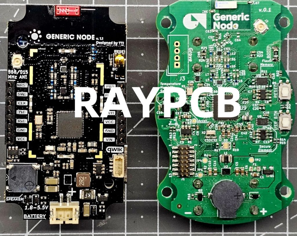
A Printed Wiring Board (PWB), also known as a Printed Circuit Board (PCB), is a fundamental component in modern electronic devices. It serves as a platform for mounting and interconnecting electronic components, such as resistors, capacitors, integrated circuits, and connectors. The PWB consists of a non-conductive substrate, typically made of fiberglass or other composite materials, with conductive traces, pads, and planes etched or printed onto its surface.
The Evolution of PWBs
The development of PWBs has been a crucial factor in the advancement of electronic devices. The history of PWBs can be traced back to the early 20th century when they were first introduced as a means to simplify and streamline the wiring of electronic components. Over the years, PWB technology has evolved significantly, enabling the creation of more complex and compact electronic devices.
| Era | Key Developments |
|---|---|
| 1900s | Invention of the printed circuit concept |
| 1920s-1930s | Development of early PCB manufacturing techniques |
| 1940s-1950s | Adoption of PCBs in military and aerospace applications |
| 1960s-1970s | Introduction of double-sided and Multilayer PCBs |
| 1980s-1990s | Advancements in PCB design software and manufacturing processes |
| 2000s-Present | Miniaturization and increased complexity of PCBs |
The Importance of PWBs in Modern Electronics
PWBs play a crucial role in the functionality, reliability, and performance of modern electronic devices. They offer several advantages over traditional point-to-point wiring methods, including:
- Compact design: PWBs allow for the dense packaging of electronic components, enabling the creation of smaller and more portable devices.
- Improved reliability: The use of PWBs reduces the risk of wiring errors and improves the overall reliability of electronic devices.
- Enhanced signal integrity: PWBs provide controlled impedance and reduced electromagnetic interference, ensuring the integrity of signals transmitted between components.
- Increased manufacturing efficiency: PWBs streamline the assembly process, allowing for automated component placement and soldering, thus reducing manufacturing time and costs.
PWB Applications
PWBs find applications in a wide range of industries and products, including:
- Consumer electronics (smartphones, laptops, televisions)
- Automotive electronics (engine control units, infotainment systems)
- Medical devices (pacemakers, imaging equipment)
- Industrial control systems (PLCs, sensors)
- Aerospace and defense (avionics, radar systems)
PWB Design Considerations
Designing a PWB involves several key considerations to ensure optimal performance, reliability, and manufacturability. Some of these considerations include:
Component Placement
The placement of components on a PWB is a critical aspect of the design process. Proper component placement ensures efficient use of board space, minimizes signal interference, and facilitates easy assembly and maintenance. Designers must consider factors such as component size, heat dissipation requirements, and signal integrity when determining the optimal placement of components on the board.
Trace Routing
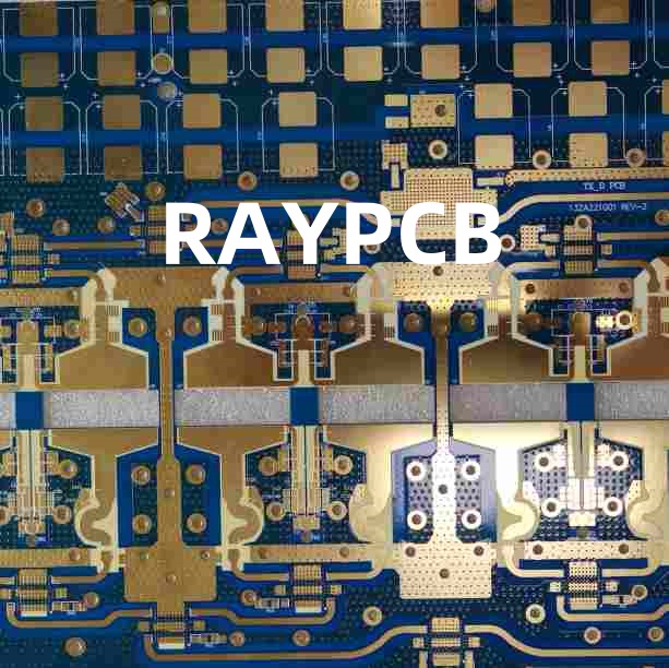
Trace routing refers to the process of creating conductive paths between components on a PWB. Designers must carefully plan the routing of traces to minimize signal interference, ensure proper signal integrity, and avoid manufacturing issues. Factors such as trace width, spacing, and impedance must be considered when routing traces on a PWB.
Layer Stack-up
Modern PWBs often consist of multiple layers, with each layer serving a specific purpose. The layer stack-up refers to the arrangement of these layers and their respective functions. A typical layer stack-up may include signal layers, power and ground planes, and dielectric layers. Designers must carefully plan the layer stack-up to ensure proper signal integrity, power distribution, and manufacturability.
Design for Manufacturing (DFM)
Design for Manufacturing (DFM) is an approach that considers the manufacturability of a PWB during the design process. DFM guidelines help designers create PWBs that are easy to manufacture, test, and assemble. By following DFM principles, designers can reduce manufacturing costs, improve yield, and ensure the overall quality of the finished product.

PWB Manufacturing Process
The manufacturing of PWBs involves several key steps, each of which plays a critical role in the quality and reliability of the final product. The typical PWB manufacturing process includes the following stages:
- PCB Design: The first step in the PWB manufacturing process is the creation of the PCB design. This involves the use of specialized software to create a digital representation of the board, including the placement of components, routing of traces, and definition of the layer stack-up.
- PCB Fabrication: Once the PCB design is complete, the fabrication process begins. This involves the creation of the physical board, typically using a subtractive process such as etching or a combination of subtractive and additive processes. The fabrication process includes the following sub-steps:
- Printing and etching of conductive traces
- Drilling of holes for component mounting and vias
- Lamination of multiple layers (for multilayer boards)
- Application of solder mask and silkscreen
- PCB Assembly: After the PCB fabrication is complete, the board moves to the assembly stage. This involves the placement and soldering of electronic components onto the board. The assembly process can be performed manually or using automated equipment, depending on the complexity of the board and the production volume.
- Testing and Inspection: Once the PCB assembly is complete, the board undergoes thorough testing and inspection to ensure proper functionality and quality. This may include visual inspections, automated optical inspections (AOI), x-ray inspections, and functional testing.
- Finishing and Packaging: After testing and inspection, the PWB may undergo additional finishing processes, such as conformal coating or potting, to enhance its durability and protection against environmental factors. Finally, the PWB is packaged and shipped to the customer.
Future Trends in PWB Technology
As electronic devices continue to evolve and become more complex, PWB technology must keep pace to meet the demands of these advanced applications. Some of the future trends in PWB technology include:
High-Density Interconnect (HDI) PCBs
High-Density Interconnect (HDI) PCBs are designed to accommodate the increasing density of electronic components in modern devices. HDI PCBs feature finer trace widths, smaller vias, and reduced layer spacing, enabling the creation of highly compact and complex boards.
Flexible and Rigid-Flex PCBs
Flexible and rigid-flex PCBs are becoming increasingly popular in applications that require flexibility, such as wearable devices and aerospace systems. These boards combine the stability of rigid PCBs with the flexibility of flexible circuits, allowing for unique form factors and improved reliability in demanding environments.
Embedded Components
Embedded components, such as resistors, capacitors, and integrated circuits, are increasingly being incorporated directly into the layers of a PWB. This approach reduces the overall size of the board, improves signal integrity, and enhances the reliability of the device.
Advanced Materials
The development of advanced materials, such as high-frequency laminates and low-loss dielectrics, is enabling the creation of PWBs that can operate at higher frequencies and withstand more extreme conditions. These materials are crucial for applications in 5G communications, automotive electronics, and aerospace systems.
Frequently Asked Questions (FAQ)
- What is the difference between a PWB and a PCB?
A PWB (Printed Wiring Board) and a PCB (Printed Circuit Board) are essentially the same things. Both terms refer to a non-conductive substrate with conductive traces, pads, and planes used to mount and interconnect electronic components. The term PWB is more commonly used in the United States, while PCB is more widely used internationally. - What are the advantages of using a PWB over point-to-point wiring?
PWBs offer several advantages over point-to-point wiring, including: - Compact design: PWBs allow for dense packaging of components, enabling smaller and more portable devices.
- Improved reliability: PWBs reduce the risk of wiring errors and improve overall reliability.
- Enhanced signal integrity: PWBs provide controlled impedance and reduced electromagnetic interference.
- Increased manufacturing efficiency: PWBs streamline the assembly process, reducing manufacturing time and costs.
- What are the key considerations when designing a PWB?
When designing a PWB, key considerations include: - Component placement: Ensuring efficient use of board space, minimizing signal interference, and facilitating easy assembly and maintenance.
- Trace routing: Carefully planning the routing of traces to minimize signal interference, ensure proper signal integrity, and avoid manufacturing issues.
- Layer stack-up: Arranging layers and their respective functions to ensure proper signal integrity, power distribution, and manufacturability.
- Design for Manufacturing (DFM): Considering the manufacturability of the PWB during the design process to reduce costs, improve yield, and ensure overall quality.
- What are the main steps in the PWB manufacturing process?
The main steps in the PWB manufacturing process are: - PCB Design: Creating a digital representation of the board using specialized software.
- PCB Fabrication: Creating the physical board through processes such as etching, drilling, lamination, and the application of solder mask and silkscreen.
- PCB Assembly: Placing and soldering electronic components onto the board.
- Testing and Inspection: Ensuring proper functionality and quality through visual inspections, automated optical inspections (AOI), x-ray inspections, and functional testing.
- Finishing and Packaging: Applying additional finishing processes, such as conformal coating or potting, and packaging the PWB for shipment.
- What are some of the future trends in PWB technology?
Some of the future trends in PWB technology include: - High-Density Interconnect (HDI) PCBs: Accommodating the increasing density of electronic components in modern devices.
- Flexible and Rigid-Flex PCBs: Combining the stability of rigid PCBs with the flexibility of flexible circuits for unique form factors and improved reliability.
- Embedded Components: Incorporating components directly into the layers of a PWB to reduce board size, improve signal integrity, and enhance reliability.
- Advanced Materials: Developing high-frequency laminates and low-loss dielectrics for PWBs that can operate at higher frequencies and withstand more extreme conditions.
No responses yet