1. Component Selection and Placement
The first step in PCB Assembly is selecting the appropriate components and placing them on the board. This process requires careful attention to several factors, including:
Component Compatibility
It is essential to ensure that the selected components are compatible with each other and with the PCB design. This includes factors such as voltage and current ratings, package sizes, and pin configurations. Using incompatible components can lead to poor performance, reliability issues, or even complete failure of the PCB.
Component Placement
The placement of components on the PCB is also critical. Components should be placed in a way that minimizes the length of the electrical connections between them, reduces the risk of electromagnetic interference (EMI), and allows for efficient heat dissipation. Proper component placement also ensures that the PCB can be easily assembled and tested.
Orientation and Polarity
Many electronic components, such as diodes, capacitors, and integrated circuits (ICs), have specific orientation and polarity requirements. Placing these components in the wrong orientation or with the wrong polarity can cause the PCB to malfunction or even damage the components.
2. Solder Paste Application
Once the components are placed on the PCB, the next step is to apply solder paste to the board. Solder paste is a mixture of tiny solder particles suspended in a flux medium, and it is used to create the electrical and mechanical connections between the components and the PCB. Proper solder paste application is critical for several reasons:
Solder Paste Volume
The volume of solder paste applied to each pad on the PCB must be carefully controlled. Too little solder paste can result in weak or incomplete solder joints, while too much solder paste can cause bridging between adjacent pads or components.
Solder Paste Consistency
The consistency of the solder paste is also important. The paste should be smooth and homogeneous, without any lumps or clumps. Inconsistent solder paste can lead to uneven solder joint formation and poor reliability.
Stencil Design
Solder paste is typically applied to the PCB using a stencil, which is a thin metal sheet with openings that correspond to the pads on the PCB. The design of the stencil is critical for ensuring that the correct amount of solder paste is applied to each pad. Stencil aperture size, shape, and orientation must be carefully designed to match the specific requirements of the PCB and components.
3. Reflow Soldering
After the solder paste is applied, the PCB is heated in a reflow oven to melt the solder particles and create the solder joints. Reflow soldering is a complex process that requires careful control of several parameters, including:
Temperature Profile
The temperature profile of the reflow oven must be carefully controlled to ensure that the solder paste melts and flows properly without damaging the components or the PCB. The temperature profile typically includes several stages, such as preheating, soaking, reflow, and cooling.
Atmosphere Control
The atmosphere inside the reflow oven must also be carefully controlled to prevent oxidation of the solder joints and to ensure proper flux activation. This typically involves using an inert gas, such as nitrogen, to displace the oxygen in the oven.
Conveyor Speed
The speed of the conveyor that carries the PCBs through the reflow oven must be carefully controlled to ensure that each PCB receives the proper amount of heat exposure. Too fast or too slow conveyor speed can result in incomplete or excessive solder joint formation.

4. Inspection and Testing
After the reflow soldering process is complete, the PCBs must be inspected and tested to ensure that they meet the required quality standards. This involves several steps, including:
Visual Inspection
The first step in PCB inspection is a visual examination of the board to check for any obvious defects, such as missing or misaligned components, solder bridges, or damaged components.
Automated Optical Inspection (AOI)
AOI is a computer-aided inspection technique that uses high-resolution cameras and image processing algorithms to detect defects on the PCB. AOI can detect a wide range of defects, including missing or misaligned components, solder bridges, insufficient or excessive solder, and component polarity errors.
X-Ray Inspection
X-ray inspection is used to detect defects that are not visible on the surface of the PCB, such as voids or cracks in the solder joints, or components that are not properly seated on the board.
Functional Testing
Functional testing involves applying power to the PCB and verifying that it performs its intended function. This can include testing individual components, such as ICs or sensors, as well as testing the overall functionality of the PCB.
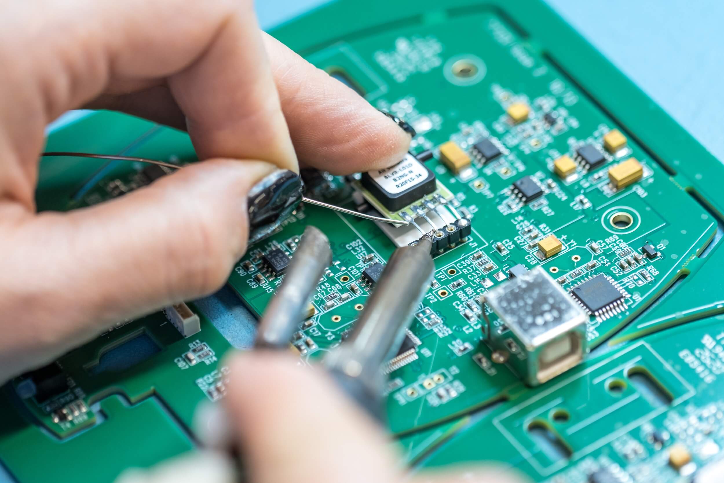
5. Rework and Repair
Despite the best efforts to ensure quality, some PCBs may still have defects that need to be corrected. Rework and repair involve identifying and correcting these defects, which can include:
Component Replacement
If a component is found to be defective or improperly placed, it may need to be removed and replaced. This can be done using specialized rework tools, such as hot air pencils or soldering irons.
Solder Joint Repair
If a solder joint is found to be weak or incomplete, it may need to be repaired. This can involve adding additional solder to the joint or using specialized repair techniques, such as solder paste dispensing or solder wire feeding.
Cleaning and Conformal Coating
After rework and repair, the PCB may need to be cleaned to remove any residual flux or other contaminants. In some cases, a conformal coating may also be applied to the PCB to provide additional protection against environmental factors, such as moisture or dust.
6. Documentation and Traceability
Finally, it is important to maintain accurate documentation and traceability throughout the PCB assembly process. This includes:
Bill of Materials (BOM)
The BOM is a list of all the components used in the PCB assembly, including part numbers, quantities, and specifications. The BOM should be reviewed and approved before the assembly process begins to ensure that all the necessary components are available and compatible.
Assembly Drawings
Assembly drawings provide a visual representation of the PCB assembly, including component placement, orientation, and polarity. These drawings should be used as a reference throughout the assembly process to ensure that the PCB is assembled correctly.
Traceability Records
Traceability records provide a link between the individual components used in the PCB assembly and the final assembled product. This includes information such as lot numbers, date codes, and supplier information. Traceability records are important for identifying and correcting any issues that may arise during the product’s lifecycle.
Quality Control Records
Quality control records document the results of the various inspection and testing steps performed during the PCB assembly process. These records provide evidence that the PCB meets the required quality standards and can be used to identify and correct any issues that may arise.
Frequently Asked Questions (FAQ)
1. What is PCB assembly?
PCB assembly is the process of assembling electronic components onto a printed circuit board (PCB) to create a functional electronic device. This process involves several steps, including component placement, solder paste application, reflow soldering, inspection, testing, and rework.
2. Why is component placement important in PCB assembly?
Component placement is important in PCB assembly because it affects the overall performance and reliability of the PCB. Proper component placement minimizes the length of electrical connections, reduces the risk of electromagnetic interference (EMI), and allows for efficient heat dissipation.
3. What is solder paste, and why is it important in PCB assembly?
Solder paste is a mixture of tiny solder particles suspended in a flux medium. It is used to create the electrical and mechanical connections between the components and the PCB. Proper solder paste application is critical for creating strong, reliable solder joints.
4. What is reflow soldering, and how does it work?
Reflow soldering is a process used in PCB assembly to melt the solder particles in the solder paste and create the solder joints. The PCB is heated in a reflow oven, which follows a carefully controlled temperature profile to melt the solder without damaging the components or the PCB.
5. Why is documentation and traceability important in PCB assembly?
Documentation and traceability are important in PCB assembly because they provide a record of the components used, the assembly process followed, and the quality control measures taken. This information is critical for identifying and correcting any issues that may arise during the product’s lifecycle and for ensuring that the PCB meets the required quality standards.
| PCB Assembly Step | Key Points |
|---|---|
| Component Selection and Placement | – Ensure component compatibility – Optimize component placement – Pay attention to orientation and polarity |
| Solder Paste Application | – Control solder paste volume – Ensure solder paste consistency – Design stencil for specific PCB requirements |
| Reflow Soldering | – Control temperature profile – Control atmosphere to prevent oxidation – Control conveyor speed for proper heat exposure |
| Inspection and Testing | – Perform visual inspection – Use automated optical inspection (AOI) – Use X-ray inspection for hidden defects – Perform functional testing |
| Rework and Repair | – Replace defective components – Repair weak or incomplete solder joints – Clean and apply conformal coating if needed |
| Documentation and Traceability | – Maintain accurate bill of materials (BOM) – Use assembly drawings as reference – Keep traceability records for components – Document quality control results |
In conclusion, PCB assembly is a complex process that requires careful attention to several key points to ensure a successful outcome. From component selection and placement to inspection and testing, each step in the process plays a critical role in the overall quality and reliability of the final product. By paying attention to these six key points and maintaining accurate documentation and traceability throughout the process, manufacturers can ensure that their PCBs meet the highest standards of quality and performance.
No responses yet