What are PCB stencils?
PCB Stencils, also known as solder paste stencils, are thin metal sheets with precise openings that correspond to the solder pad locations on a PCB. These stencils are used to apply solder paste onto the PCB’s surface, ensuring accurate and consistent solder paste deposition. The stencil acts as a template, allowing the solder paste to be applied only to the desired areas of the PCB, which is crucial for the proper placement and soldering of surface mount components.
Types of PCB Stencils
There are several types of PCB stencils available, each with its own unique characteristics and advantages. The most common types include:
Laser-Cut Stencils
Laser-cut stencils are created using high-precision laser cutting technology. The laser beam cuts the stencil’s openings according to the PCB’s design, resulting in clean, accurate, and burr-free apertures. Laser-cut stencils are known for their high level of precision and are suitable for a wide range of PCB Designs, including those with fine-pitch components.
Electroformed Stencils
Electroformed stencils are manufactured using an electroplating process, where a thin layer of metal (usually nickel) is deposited onto a photoresist-coated master. This process allows for the creation of stencils with extremely fine apertures and smooth walls, making them ideal for high-density PCB designs with very small components.
Chemically Etched Stencils
Chemically etched stencils are produced by selectively etching away metal from a sheet using a chemical process. This method is less precise compared to laser cutting or electroforming, but it is more cost-effective for larger apertures and simpler PCB designs.
3D-Printed Stencils
3D-printed stencils are a relatively new addition to the PCB stencil family. These stencils are created using additive manufacturing techniques, allowing for the production of complex and customized stencil designs. While not as common as laser-cut or electroformed stencils, 3D-printed stencils offer unique advantages in terms of design flexibility and rapid prototyping.

Stencil Materials
PCB stencils can be made from various materials, each with its own properties and benefits. The most common stencil materials include:
Stainless Steel
Stainless steel is the most widely used material for PCB stencils due to its durability, stability, and resistance to corrosion. Stainless steel stencils are suitable for multiple printing cycles and can withstand the rigors of the PCB Assembly process.
Nickel
Nickel stencils are known for their excellent Surface Finish and high-resolution capabilities. They are often used for electroformed stencils, where the smooth walls and fine apertures are critical for precise solder paste deposition.
Polyimide
Polyimide stencils, also known as plastic stencils, are a cost-effective alternative to metal stencils. They are lightweight, flexible, and suitable for low-volume production or prototyping. However, polyimide stencils have a shorter lifespan compared to metal stencils and may not be suitable for high-precision applications.

Stencil Thickness
The thickness of a PCB stencil plays a crucial role in determining the amount of solder paste deposited onto the PCB. The most common stencil thicknesses are:
| Thickness (mm) | Thickness (mils) | Typical Applications |
|---|---|---|
| 0.100 | 4 | Standard SMT components |
| 0.125 | 5 | Fine-pitch components |
| 0.150 | 6 | High-volume solder paste deposition |
| 0.200 | 8 | Power components and connectors |
The choice of stencil thickness depends on various factors, such as the size and pitch of the components, the desired solder paste volume, and the PCB’s design. Thinner stencils are generally used for smaller, fine-pitch components, while thicker stencils are employed for larger components or when a higher solder paste volume is required.

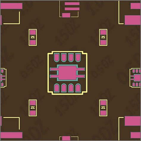
Stencil Aperture Design
The design of the stencil apertures is critical for ensuring proper solder paste deposition and preventing defects such as bridging or insufficient solder. There are several factors to consider when designing stencil apertures:
Aperture Size
The size of the stencil apertures should be carefully calculated based on the size of the solder pads on the PCB. Generally, the aperture size is slightly smaller than the solder pad to account for the solder paste’s tendency to spread during the reflow process. The aperture size is typically expressed as a percentage of the solder pad size, with common values ranging from 80% to 100%.
Aperture Shape
Stencil apertures can have various shapes, depending on the solder pad design and the desired solder paste deposition. Common aperture shapes include:
- Square: Used for standard SMT pads
- Rectangular: Used for elongated pads or connectors
- Circular: Used for round pads, such as those found on BGA components
- D-shaped: Used for pads with a specific orientation or polarity
The choice of aperture shape should be based on the specific requirements of the PCB design and the components being used.
Aperture Orientation
The orientation of the stencil apertures should match the orientation of the solder pads on the PCB. This ensures that the solder paste is deposited in the correct location and orientation, facilitating proper component placement and soldering.
Stencil Frame and Mounting
PCB stencils are typically mounted on a frame to ensure stability and ease of handling during the printing process. The most common types of stencil frames are:
Aluminum Frames
Aluminum frames are lightweight, durable, and cost-effective. They are suitable for most PCB stencil applications and are easy to handle and store.
Magnetic Frames
Magnetic frames use magnets to secure the stencil in place, allowing for quick and easy stencil changes. These frames are particularly useful in high-volume production environments where frequent stencil changes are required.
Frameless Stencils
Frameless stencils, also known as foil stencils, are thin, flexible stencils that do not require a frame. They are typically used for low-volume production or prototype runs, where the cost and setup time of a framed stencil may not be justified.
Stencil Printing Process
The stencil printing process involves several key steps to ensure accurate and consistent solder paste deposition:
-
Stencil Alignment: The stencil is aligned with the PCB using fiducial marks or other alignment features. Proper alignment is crucial for ensuring that the solder paste is deposited in the correct locations on the PCB.
-
Solder Paste Application: Solder paste is applied to the top surface of the stencil, typically using a automated solder paste dispenser or a manual squeegee.
-
Solder Paste Deposition: The squeegee is used to spread the solder paste across the stencil, forcing it through the apertures and onto the solder pads on the PCB. The squeegee pressure, speed, and angle are carefully controlled to ensure even and consistent solder paste deposition.
-
Stencil Removal: After the solder paste has been deposited, the stencil is carefully lifted away from the PCB, leaving the solder paste in the desired locations.
-
Inspection: The PCB is inspected to ensure that the solder paste has been properly deposited and that there are no defects, such as bridging or insufficient solder.
Stencil Cleaning and Maintenance
Regular cleaning and maintenance of PCB stencils are essential for ensuring consistent and high-quality solder paste deposition. Stencils should be cleaned after each use to remove any residual solder paste, flux, or debris that may clog the apertures or affect the printing quality.
There are several methods for cleaning PCB stencils, including:
- Manual cleaning with solvents and wiping materials
- Automated stencil cleaning systems that use ultrasonic, spray, or vapor degreasing techniques
- Stencil understencil wiping systems that clean the bottom side of the stencil during the printing process
In addition to regular cleaning, stencils should be periodically inspected for signs of wear, damage, or aperture clogging. Damaged or worn stencils should be repaired or replaced to maintain printing quality and prevent defects.
PCB Stencil Costs
The cost of PCB stencils varies depending on several factors, such as the stencil type, material, thickness, size, and complexity of the design. Generally, laser-cut and electroformed stencils are more expensive than chemically etched or 3D-printed stencils due to their higher precision and the specialized equipment required for their production.
The following table provides a rough cost comparison for different types of PCB stencils:
| Stencil Type | Relative Cost |
|---|---|
| Laser-cut | High |
| Electroformed | High |
| Chemically Etched | Medium |
| 3D-Printed | Low to Medium |
It is important to note that the cost of a PCB stencil is a relatively small portion of the overall PCB assembly cost, and investing in a high-quality stencil can yield significant benefits in terms of solder paste deposition accuracy, consistency, and reduced defects.
Frequently Asked Questions (FAQ)
-
What is the difference between a solder paste stencil and a solder mask?
A solder paste stencil is used to apply solder paste onto the PCB’s surface, while a solder mask is a protective layer applied to the PCB that prevents solder from adhering to non-pad areas. -
Can I reuse a PCB stencil?
Yes, PCB stencils can be reused multiple times with proper cleaning and maintenance. However, the stencil’s lifespan will depend on factors such as the material, thickness, and frequency of use. -
How do I choose the right stencil thickness for my PCB?
The choice of stencil thickness depends on the size and pitch of the components, the desired solder paste volume, and the PCB’s design. Consult with your stencil manufacturer or PCB assembly provider to determine the optimal stencil thickness for your specific application. -
What is the advantage of using a frameless stencil?
Frameless stencils, or foil stencils, are thinner and more flexible than framed stencils, making them easier to handle and store. They are also more cost-effective for low-volume production or prototype runs. -
How often should I clean my PCB stencil?
PCB stencils should be cleaned after each use to remove any residual solder paste, flux, or debris. Regular cleaning helps maintain the stencil’s performance and longevity, and prevents defects caused by clogged apertures or contamination.
Conclusion
PCB stencils are a critical component in the electronics manufacturing process, enabling the precise and consistent application of solder paste onto PCBs. By understanding the various types, materials, thicknesses, and aperture designs of PCB stencils, as well as the stencil printing process and maintenance requirements, manufacturers can optimize their PCB assembly operations and produce high-quality, reliable electronic products.
Investing in the right PCB stencil for a given application, along with proper handling, cleaning, and maintenance, can yield significant benefits in terms of solder paste deposition accuracy, reduced defects, and overall PCB assembly efficiency. As the electronics industry continues to evolve, with ever-increasing demands for miniaturization and high-density PCB designs, the importance of PCB stencils in ensuring manufacturing success will only continue to grow.
No responses yet