Introduction to PCB stencils
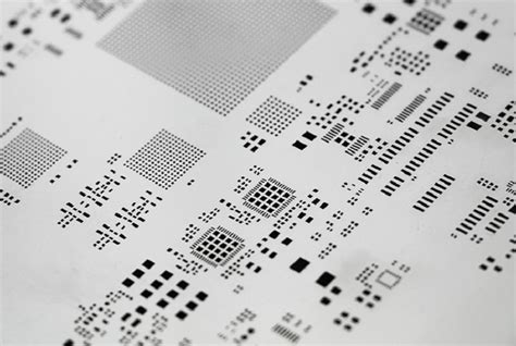
A PCB (printed circuit board) stencil is a thin sheet of material, typically stainless steel or polyester, that is used to apply solder paste onto a PCB during the assembly process. The stencil has apertures or openings that correspond to the pads on the PCB where solder paste needs to be deposited.
PCB Stencils play a crucial role in the surface mount technology (SMT) assembly process, ensuring precise and consistent solder paste application. This leads to better solder joints, fewer defects, and higher quality PCB Assembly.
How PCB Stencils Work
PCB stencils work by allowing solder paste to be deposited onto the PCB pads through the openings in the stencil. The process involves the following steps:
- Solder paste is placed on top of the stencil.
- A squeegee blade is used to spread the solder paste across the stencil, forcing it through the openings and onto the PCB pads.
- The stencil is then lifted away, leaving precise deposits of solder paste on the pads.
- The PCB is ready for component placement and reflow soldering.
The thickness of the stencil and the size of the apertures determine the amount of solder paste deposited on each pad. It is essential to choose the right stencil thickness and aperture size based on the specific requirements of the PCB design and components used.

Types of PCB Stencils
There are two main types of PCB stencils: stainless steel and polyester. Each type has its own advantages and disadvantages.
Stainless Steel Stencils
Stainless steel stencils are the most common type used in PCB assembly. They offer several benefits:
- Durability: Stainless steel stencils are robust and can withstand repeated use without deformation or wear.
- Precision: Stainless steel allows for very fine apertures and tight tolerances, making it suitable for high-density PCB designs.
- Compatibility: Stainless steel is compatible with a wide range of solder paste formulations.
However, stainless steel stencils also have some drawbacks:
- Cost: They are more expensive than polyester stencils.
- Cleaning: Stainless steel stencils require thorough cleaning after each use to prevent solder paste buildup and contamination.
Polyester Stencils
Polyester stencils, also known as mesh or screen stencils, are an alternative to stainless steel. They have the following advantages:
- Cost-effective: Polyester stencils are less expensive than stainless steel stencils.
- Flexibility: The flexible nature of polyester allows the stencil to conform to slightly uneven PCB surfaces.
- Ease of use: Polyester stencils are lighter and easier to handle than stainless steel stencils.
However, polyester stencils also have some limitations:
- Durability: They are less durable than stainless steel and may stretch or deform over time.
- Resolution: Polyester stencils cannot achieve the same fine pitch and high resolution as stainless steel stencils.

Stencil Thickness and Aperture Size
Choosing the right stencil thickness and aperture size is crucial for achieving optimal solder paste deposition and solder joint quality. The stencil thickness determines the volume of solder paste deposited, while the aperture size controls the area over which the paste is deposited.
Stencil Thickness
The most common stencil thicknesses used in PCB assembly are:
- 0.1 mm (4 mil)
- 0.12 mm (5 mil)
- 0.15 mm (6 mil)
- 0.2 mm (8 mil)
Thinner stencils (0.1 mm and 0.12 mm) are typically used for fine-pitch components and high-density PCB designs. Thicker stencils (0.15 mm and 0.2 mm) are used for larger components and PCBs with greater solder volume requirements.
| Stencil Thickness | Typical Use |
|---|---|
| 0.1 mm (4 mil) | Fine-pitch components, high-density PCBs |
| 0.12 mm (5 mil) | Fine-pitch components, high-density PCBs |
| 0.15 mm (6 mil) | General-purpose PCB assembly |
| 0.2 mm (8 mil) | Large components, high solder volume |
Aperture Size
The aperture size in a PCB stencil is typically designed to be slightly larger than the pad size on the PCB. This allows for some tolerance in the alignment between the stencil and the PCB, ensuring that the solder paste is deposited accurately on the pads.
The aperture size is usually expressed as a percentage of the pad size. Common aperture size guidelines are:
- Fine-pitch components (pitch < 0.5 mm): 80-90% of pad size
- Standard components (pitch 0.5-1.0 mm): 90-100% of pad size
- Large components (pitch > 1.0 mm): 100-120% of pad size
It is important to note that these are general guidelines, and the actual aperture size may need to be adjusted based on factors such as the specific solder paste being used, the PCB material, and the reflow soldering profile.

Stencil Design and Fabrication
Designing and fabricating a PCB stencil involves several key considerations to ensure optimal performance and compatibility with the PCB assembly process.
Stencil Design
The stencil design process begins with the PCB Layout data, typically in Gerber format. The stencil designer uses this data to create a stencil layout that includes:
- Aperture locations and sizes
- Fiducial marks for alignment
- Stencil thickness
- Border and frame design
The stencil design must take into account the specific requirements of the PCB, such as the Component Types, pitch, and solder volume needs. It is also essential to consider the capabilities of the stencil fabrication process and the solder paste application equipment to be used.
Stencil Fabrication
PCB stencils are typically fabricated using one of two methods: laser cutting or chemical etching.
Laser Cutting
Laser cutting is the most common method for fabricating stainless steel stencils. A high-precision laser is used to cut the apertures and other features into the stencil material. Laser cutting offers several advantages:
- High accuracy and repeatability
- Ability to create very fine apertures and intricate designs
- Rapid turnaround times
Chemical Etching
Chemical etching is an alternative method for fabricating stainless steel stencils. In this process, the stencil design is transferred onto the stainless steel sheet using a photoresist, and then the unwanted material is removed using a chemical etchant. Chemical etching has some advantages:
- Lower cost for large quantities
- Ability to create complex aperture shapes
However, chemical etching also has some limitations compared to laser cutting:
- Lower accuracy and repeatability
- Longer turnaround times
- Difficulty achieving very fine apertures
Stencil Maintenance and Cleaning
Proper maintenance and cleaning of PCB stencils are essential for ensuring consistent solder paste deposition and preventing defects in the PCB assembly process.
Stencil Cleaning
Solder paste residue can build up on the stencil over time, leading to clogged apertures and inconsistent solder paste deposition. Regular cleaning of the stencil is necessary to maintain its performance. There are two main methods for cleaning PCB stencils:
-
Manual cleaning: This involves using solvents and wiping the stencil by hand to remove solder paste residue. Manual cleaning is suitable for small-scale production or when the stencil is not heavily contaminated.
-
Automated cleaning: Automated stencil cleaning systems use a combination of solvents, brushes, and high-pressure sprays to clean the stencil. This method is more efficient and thorough than manual cleaning and is recommended for high-volume production.
Regardless of the cleaning method used, it is important to use compatible solvents that effectively remove solder paste residue without damaging the stencil material.
Stencil Storage
Proper storage of PCB stencils is crucial for maintaining their quality and preventing damage. Stencils should be stored in a clean, dry environment, away from direct sunlight and extreme temperatures. It is also recommended to store stencils vertically to prevent warping or deformation.
When not in use, stencils should be protected with a cover or placed in a sealed container to prevent contamination and damage. Regularly inspecting stencils for signs of wear, damage, or contamination can help prolong their life and ensure consistent performance.
Benefits of Using PCB Stencils
Using PCB stencils in the SMT Assembly process offers several significant benefits:
-
Consistency: Stencils ensure consistent solder paste deposition across the PCB, reducing the risk of defects caused by insufficient or excessive solder.
-
Efficiency: Stencil printing is a fast and efficient method for applying solder paste to a large number of pads simultaneously, reducing assembly time and increasing throughput.
-
Precision: Stencils enable precise control over the amount and placement of solder paste, which is essential for achieving reliable solder joints, especially for fine-pitch components.
-
Cost-effectiveness: By reducing solder paste waste and minimizing defects, stencils contribute to lower overall assembly costs.
-
Scalability: Stencil printing is a scalable process that can be easily adapted to various production volumes, from prototyping to high-volume manufacturing.
Troubleshooting Common Stencil Issues
Despite the benefits of using PCB stencils, several issues can arise during the stencil printing process. Some common problems and their solutions include:
-
Insufficient solder paste deposition: This can be caused by clogged apertures, low stencil pressure, or incorrect aperture size. Cleaning the stencil, adjusting the pressure, or modifying the aperture design can help resolve this issue.
-
Excessive solder paste deposition: Overly large apertures, high stencil pressure, or slow squeegee speed can lead to excessive solder paste deposition. Adjusting these parameters or reducing the stencil thickness can help mitigate this problem.
-
Solder paste smearing: This can occur when the squeegee blade is worn or the stencil is not properly aligned with the PCB. Replacing the squeegee blade or improving the alignment process can prevent solder paste smearing.
-
Stencil damage: Improper handling, storage, or cleaning can lead to stencil damage, such as bent or stretched areas. Following proper maintenance and storage procedures can help prevent damage and prolong the stencil’s life.
Frequently Asked Questions (FAQ)
1. How often should I clean my PCB stencil?
The frequency of cleaning depends on factors such as the solder paste type, production volume, and environmental conditions. As a general rule, stencils should be cleaned every 4-8 hours of continuous use or whenever print quality degrades. In high-humidity environments or when using no-clean solder pastes, more frequent cleaning may be necessary.
2. Can I reuse a PCB stencil for different PCB designs?
While it is possible to reuse a stencil for different PCB designs, it is generally not recommended. Each PCB design has unique pad layouts and solder volume requirements, which necessitate a specific stencil design. Using a stencil designed for one PCB on a different PCB can lead to poor solder paste deposition and defects.
3. How do I choose the right solder paste for my stencil printing process?
Selecting the right solder paste depends on factors such as the component types, PCB material, and reflow soldering profile. The solder paste should have a particle size and viscosity compatible with the stencil aperture sizes and printing equipment. It is also essential to consider the flux activity, alloy composition, and shelf life of the solder paste. Consult with your solder paste supplier or stencil manufacturer for guidance on selecting the best solder paste for your specific application.
4. What is the typical lifespan of a PCB stencil?
The lifespan of a PCB stencil depends on various factors, including the stencil material, cleaning frequency, and handling practices. Stainless steel stencils can typically last for 50,000 to 100,000 prints with proper maintenance and storage. Polyester stencils have a shorter lifespan, usually around 5,000 to 10,000 prints. Regular inspection and replacement of worn or damaged stencils are essential for maintaining print quality and avoiding defects.
5. Can I use a PCB stencil for hand soldering?
While PCB stencils are primarily used for solder paste application in the SMT assembly process, they can also be used for hand soldering. A stencil can be used to apply solder paste to the pads, and then components can be placed and soldered using a soldering iron. This technique can be useful for prototyping or low-volume assembly. However, hand soldering with a stencil requires skill and practice to achieve consistent results, and it may not be suitable for all component types or PCB designs.
Conclusion
PCB stencils are an essential tool in the SMT assembly process, enabling precise and consistent solder paste application for reliable solder joints and high-quality PCB assembly. By understanding the types of stencils, their design and fabrication processes, and proper maintenance and troubleshooting techniques, PCB manufacturers and assemblers can optimize their stencil printing process and achieve better results.
As PCB designs continue to evolve with smaller components and higher densities, the importance of PCB stencils will only grow. Keeping up with the latest stencil technologies, materials, and best practices is crucial for staying competitive in the fast-paced world of electronics manufacturing.
No responses yet