Introduction to DRC and Kicad
Kicad is a popular open-source electronic design automation (EDA) software that allows users to design printed circuit boards (PCBs). One of the essential features of Kicad is the Design Rule Check (DRC), which helps identify potential issues in the PCB Layout before manufacturing. DRC ensures that the design adheres to the predefined rules and constraints, minimizing the chances of errors and reducing the overall cost of production.
However, users may encounter issues with DRC when working with ground planes in Kicad. This article will discuss the common problems related to DRC and Kicad ground planes, along with their solutions.
What is a Ground Plane?
A ground plane is a large copper area on a PCB that serves as a low-impedance return path for electrical currents. It helps to reduce electromagnetic interference (EMI), provides shielding, and improves signal integrity. Ground planes are essential in high-speed digital designs and analog circuits.
Importance of DRC in PCB Design
DRC is a crucial step in the PCB design process. It helps to identify and resolve issues such as:
- Shorts and opens
- Clearance violations
- Trace width and spacing violations
- Copper pour and thermal relief issues
By running DRC, designers can ensure that their PCB layout is manufacturable and meets the required specifications.
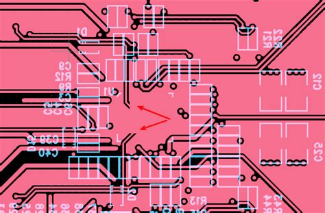
Common Issues with DRC and Kicad Ground Plane
1. Incorrect Net Assignments
One of the most common issues with DRC and ground planes in Kicad is incorrect net assignments. If the ground plane is not properly connected to the ground net, DRC will report errors such as unconnected copper areas or floating copper.
To resolve this issue:
- Ensure that the ground plane is assigned to the correct net (usually named “GND”).
- Check the net class settings to verify that the ground net is included in the appropriate net class.
- Inspect the PCB layout for any missing or incorrect connections between the ground plane and ground pads.
2. Insufficient Clearance
Another common issue is insufficient clearance between the ground plane and other components or traces. DRC may report clearance violations if the spacing between the ground plane and other elements is less than the specified minimum.
To resolve this issue:
- Review the clearance settings in the DRC rules and adjust them if necessary.
- Modify the PCB layout to ensure adequate spacing between the ground plane and other components or traces.
- Use the “Edit Copper Pour” tool to manually adjust the ground plane shape and clearance.
3. Thermal Relief Issues
Thermal relief is a technique used to improve solderability and prevent heat damage to components during the soldering process. However, incorrect thermal relief settings can lead to DRC errors.
To resolve this issue:
- Check the thermal relief settings in the DRC rules and ensure they are appropriate for your design.
- Verify that the thermal relief connections are properly placed and sized.
- Use the “Rebuild Thermal Relief Connections” tool to update the thermal relief connections after making changes to the ground plane or component placement.
4. Copper Pour Issues
Copper pour is the process of filling empty areas on the PCB with copper to create a ground plane. Issues with copper pour settings can result in DRC errors.
To resolve this issue:
- Review the copper pour settings in the “Copper Pour Properties” dialog and adjust them if necessary.
- Ensure that the copper pour is assigned to the correct net (usually “GND”).
- Use the “Rebuild Copper Pour” tool to update the ground plane after making changes to the PCB layout.
5. Incomplete or Outdated DRC Rules
Incomplete or outdated DRC rules can lead to false positives or false negatives in the DRC report. It is essential to maintain an up-to-date and comprehensive set of DRC rules tailored to your specific design requirements and manufacturing capabilities.
To resolve this issue:
- Regularly review and update the DRC rules to ensure they are complete and accurate.
- Consult with your PCB manufacturer to obtain their recommended DRC rules and incorporate them into your Kicad project.
- Use the “DRC Clearance Matrix” to define specific clearance requirements between different net classes or component types.

Best Practices for Avoiding DRC Issues with Ground Planes
To minimize the occurrence of DRC issues related to ground planes in Kicad, follow these best practices:
- Assign nets correctly: Ensure that all ground connections are assigned to the appropriate ground net (usually “GND”). Double-check the net assignments for components, pads, and traces.
- Define proper clearance rules: Set up appropriate clearance rules in the DRC settings to maintain adequate spacing between the ground plane and other elements. Consider the manufacturing capabilities and design requirements when defining clearance values.
- Use appropriate thermal relief settings: Configure thermal relief settings based on the component types and soldering process. Ensure that thermal relief connections are properly placed and sized.
- Optimize copper pour settings: Adjust copper pour settings to achieve the desired ground plane coverage and performance. Consider factors such as minimum width, clearance, and thermal relief.
- Regularly update DRC rules: Keep the DRC rules up-to-date and tailored to your specific design requirements and manufacturing capabilities. Consult with your PCB manufacturer and incorporate their recommended DRC rules.
- Perform frequent DRC checks: Run DRC checks regularly during the PCB layout process to identify and resolve issues early. This approach saves time and effort in the long run.
- Review and refine the PCB layout: Visually inspect the PCB layout for any obvious issues or inconsistencies related to the ground plane. Make necessary adjustments to improve the layout and resolve DRC errors.

Frequently Asked Questions (FAQ)
- Q: What is the purpose of a ground plane in PCB design?
A: A ground plane serves as a low-impedance return path for electrical currents, reduces electromagnetic interference (EMI), provides shielding, and improves signal integrity. - Q: Why is DRC important in PCB design?
A: DRC helps identify and resolve issues such as shorts, opens, clearance violations, trace width and spacing violations, and copper pour and thermal relief issues. It ensures that the PCB layout is manufacturable and meets the required specifications. - Q: How can I resolve incorrect net assignments for ground planes in Kicad?
A: To resolve incorrect net assignments, ensure that the ground plane is assigned to the correct net (usually “GND”), check the net class settings, and inspect the PCB layout for any missing or incorrect connections. - Q: What should I do if DRC reports insufficient clearance between the ground plane and other elements?
A: Review the clearance settings in the DRC rules and adjust them if necessary. Modify the PCB layout to ensure adequate spacing between the ground plane and other components or traces. Use the “Edit Copper Pour” tool to manually adjust the ground plane shape and clearance. - Q: How can I avoid DRC issues related to ground planes in Kicad?
A: To avoid DRC issues, assign nets correctly, define proper clearance rules, use appropriate thermal relief settings, optimize copper pour settings, regularly update DRC rules, perform frequent DRC checks, and review and refine the PCB layout.
Conclusion
DRC is a critical step in the PCB design process, and issues related to ground planes can lead to manufacturing problems and reduced performance. By understanding the common issues with DRC and Kicad ground planes, designers can take appropriate measures to resolve them and ensure a robust and manufacturable PCB layout.
By following best practices such as correct net assignments, proper clearance rules, appropriate thermal relief settings, optimized copper pour settings, and regular DRC checks, designers can minimize the occurrence of DRC issues and streamline the PCB design process.
Remember to consult with your PCB manufacturer and incorporate their recommended DRC rules to ensure compatibility with their manufacturing capabilities. Regularly reviewing and refining the PCB layout, along with frequent DRC checks, will help identify and resolve issues early, saving time and effort in the long run.
By addressing DRC issues related to ground planes and adopting best practices, Kicad users can create high-quality PCB designs that meet performance requirements and are ready for manufacturing.
No responses yet