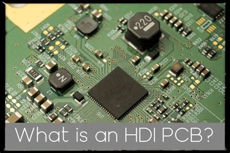
What is an HDI PCB?
An HDI (High Density Interconnect) PCB is a printed circuit board with a higher wiring density per unit area than conventional PCBs. This is achieved by incorporating narrower traces and spaces (<100 μm), smaller vias (< 150 μm), and capture pads (<400 μm), and by using a sequential lamination fabrication process to achieve higher layer counts.
HDI PCBs offer several advantages over traditional PCB designs:
- Miniaturization and weight reduction
- Improved electrical performance
- Lower power consumption
- Higher signal integrity
- Increased reliability
As electronic devices continue to shrink in size and grow in complexity, HDI PCBs have become an essential technology for a wide range of industries, from consumer electronics and telecommunications to aerospace and medical devices.
HDI PCB Classifications
HDI PCBs are classified based on the density of their interconnects and the fabrication technologies used. The most common HDI classifications are:
| Class | Via Type | Trace/Space (μm) | Capture Pad (μm) | Layers |
|---|---|---|---|---|
| HDI | μVia | 75/75 | 350 | 8-16 |
| ADHDI | μVia | 50/50 | 250 | 8-24 |
| AHDBI | μVia | 30/30 | 150 | 10-36 |
- HDI (High Density Interconnect): The most common HDI class, with trace/space widths of 75/75 μm and capture pads of 350 μm.
- ADHDI (Advanced HDI): Offers higher density than standard HDI, with trace/space widths of 50/50 μm and capture pads of 250 μm.
- AHDBI (Any Layer HDI): The highest density HDI class, with trace/space widths of 30/30 μm and capture pads of 150 μm, enabling HDI features on any layer of the PCB.

HDI PCB Stackup Design
A well-designed stackup is crucial for achieving a high-quality HDI PCB. The stackup determines the number of layers, the arrangement of signal, power, and ground planes, and the placement of vias and microvia structures.
Microvia Structures
Microvias are small, laser-drilled vias that enable high-density interconnects between layers. There are several types of microvia structures used in HDI PCBs:
- Blind vias: Connect an outer layer to an inner layer, but do not go through the entire board.
- Buried vias: Connect inner layers to each other, but do not reach the outer layers.
- Stacked vias: Multiple microvias stacked on top of each other to connect several layers.
- Staggered vias: Microvias that are offset from each other to avoid stacking.
Sequential Lamination
HDI PCBs are typically fabricated using a sequential lamination process, where the layers are built up one at a time. This allows for the incorporation of microvia structures and enables higher layer counts compared to traditional PCBs.
A typical HDI stackup might consist of:
- Core layers: The central layers of the PCB, usually a thick, rigid material.
- Build-up layers: The outer layers of the PCB, added sequentially using a thin, flexible material.
- Microvia layers: Layers containing blind, buried, or staggered microvias for high-density interconnects.

HDI PCB Material Selection
Choosing the right materials is essential for ensuring the performance, reliability, and manufacturability of an HDI PCB. The key considerations for HDI material selection include:
Dielectric Materials
The dielectric material determines the insulation between conductive layers and affects the PCB’s electrical properties. Common dielectric materials for HDI PCBs include:
- FR-4: A standard, cost-effective material with good mechanical and electrical properties.
- Polyimide: A high-performance material with excellent thermal stability and low dielectric loss.
- Rogers: A specialty material with low dielectric constant and loss, ideal for high-frequency applications.
Copper Foils
The copper foil thickness and type affect the PCB’s signal integrity and current-carrying capacity. HDI PCBs typically use thinner copper foils (1/2 oz. or less) to enable finer traces and spaces. Electrodeposited (ED) copper foils are preferred for their smooth surface finish and superior adhesion.
Solder Mask
The solder mask protects the copper traces from oxidation and prevents solder bridging during assembly. HDI PCBs require high-resolution solder masks with good registration accuracy to ensure proper coverage of the fine features.

HDI PCB Design Considerations
Designing an HDI PCB requires careful consideration of several factors to ensure optimal performance and manufacturability:
Signal Integrity
Maintaining good signal integrity is critical in HDI PCBs, where high-speed signals are routed through dense interconnects. Key strategies for improving signal integrity include:
- Impedance control: Matching the impedance of the traces to the source and load to minimize reflections.
- Length matching: Ensuring that critical signal paths have equal lengths to minimize skew.
- Shielding: Using ground planes and via shielding to reduce crosstalk and electromagnetic interference (EMI).
Thermal Management
HDI PCBs often have high power densities, which can lead to thermal issues if not properly managed. Effective thermal management strategies include:
- Copper pours: Using large copper areas to dissipate heat from high-power components.
- Thermal vias: Placing vias near hot components to transfer heat to inner layers or the opposite side of the board.
- Materials: Choosing materials with high thermal conductivity, such as metal-core PCBs or thermally enhanced dielectrics.
DFM (Design for Manufacturability)
Designing an HDI PCB with manufacturability in mind helps to ensure a smooth, cost-effective production process. Key DFM considerations include:
- Minimum feature sizes: Adhering to the manufacturer’s minimum trace, space, and via sizes to avoid yield issues.
- Pad and via design: Using properly sized and shaped pads and vias to ensure reliable connections and prevent manufacturing defects.
- Panelization: Designing the PCB to fit efficiently on a standard panel size to minimize material waste and production costs.
HDI PCB Manufacturing Process
The manufacturing process for HDI PCBs is more complex than that of traditional PCBs due to the high density of features and the use of sequential lamination. The main steps in HDI PCB manufacturing are:
- Core lamination: The core layers are laminated together using heat and pressure.
- Drilling: Through-holes and blind vias are drilled in the core layers.
- Plating: The drilled holes are plated with copper to create conductive pathways.
- Patterning: The outer layers are patterned using photolithography and etching.
- Sequential lamination: The build-up layers are added one at a time, with microvias drilled and plated in between each layer.
- Surface finish: A surface finish, such as ENIG (Electroless Nickel Immersion Gold) or OSP (Organic Solderability Preservative), is applied to protect the copper and improve solderability.
- Solder mask: The solder mask is applied and patterned to protect the traces and prevent solder bridging.
- Silkscreen: The silkscreen is applied to add component designators, logos, and other markings.
- Electrical test: The completed HDI PCB is tested for continuity, shorts, and opens to ensure functionality.
Quality Control and Testing
Ensuring the quality and reliability of HDI PCBs requires rigorous quality control and testing throughout the manufacturing process. Some key quality control measures include:
- Automated optical inspection (AOI): Using machine vision to check for defects such as shorts, opens, and misaligned features.
- X-ray inspection: Using X-rays to check for internal defects such as voids, delamination, and barrel cracks.
- Electrical testing: Performing continuity, insulation resistance, and high-potential (hipot) tests to verify electrical performance.
- Microsectioning: Cross-sectioning a sample of the PCBs to inspect the internal structure and verify the integrity of vias and plating.
- Thermal cycling: Subjecting the PCBs to temperature extremes to ensure reliability under varying environmental conditions.
HDI PCB Assembly Considerations
Assembling HDI PCBs requires specialized equipment and processes to accommodate the high density of components and interconnects. Some key considerations for HDI PCB assembly include:
- Surface mount technology (SMT): HDI PCBs are typically assembled using SMT, which involves placing and soldering components directly onto the surface of the board.
- Fine-pitch components: HDI PCBs often incorporate fine-pitch components, such as ball grid arrays (BGAs) and quad flat no-leads (QFNs), which require precise placement and soldering.
- Reflow soldering: Reflow soldering is the preferred method for HDI PCB assembly, as it allows for the simultaneous soldering of multiple components in a controlled environment.
- Underfill: Some fine-pitch components, such as BGAs, require underfill to reinforce the solder joints and improve reliability.
- Inspection: Post-assembly inspection, such as X-ray and AOI, is critical for ensuring the quality and reliability of the assembled HDI PCB.
Troubleshooting and Rework
Despite careful design and manufacturing, issues can still arise during HDI PCB production and assembly. Common problems and their solutions include:
- Shorts and opens: Shorts can be caused by overplating, solder bridging, or conductive debris, while opens can result from underplating, broken traces, or poor solder joints. These issues can often be resolved by selective rework, such as manually removing the short or adding a jumper wire to bypass the open.
- Delamination: Delamination can occur due to poor bonding between layers, thermal stress, or mechanical damage. In some cases, delamination can be repaired by injecting epoxy into the affected area and curing it under pressure.
- Component failure: Components can fail due to defects, overcurrent, or electrostatic discharge (ESD). Replacing the failed component requires careful desoldering and soldering to avoid damaging the surrounding area.
Future Trends in HDI PCBs
As electronic devices continue to advance, HDI PCBs will need to keep pace with new technologies and requirements. Some future trends in HDI PCBs include:
- Smaller features: The demand for even smaller and more compact devices will drive the development of HDI PCBs with finer traces, spaces, and microvias.
- Higher frequencies: The increasing use of high-frequency technologies, such as 5G and millimeter-wave, will require HDI PCBs with improved signal integrity and low-loss materials.
- Embedded components: Embedding active and passive components within the layers of the HDI PCB can further increase density and reduce size.
- 3D packaging: Stacking multiple HDI PCBs in a 3D package can enable even higher densities and more complex functionalities.
- Flexible and stretchable: The growing demand for wearable and implantable electronics will drive the development of flexible and stretchable HDI PCBs that can conform to the human body.
Frequently Asked Questions (FAQ)
- What is the difference between an HDI PCB and a traditional PCB?
-
HDI PCBs have a higher wiring density per unit area than traditional PCBs, achieved through finer traces and spaces, smaller vias and capture pads, and the use of microvias and sequential lamination.
-
What are the benefits of using an HDI PCB?
-
HDI PCBs offer several benefits, including miniaturization, weight reduction, improved electrical performance, lower power consumption, higher signal integrity, and increased reliability.
-
What industries commonly use HDI PCBs?
-
HDI PCBs are used in a wide range of industries, including consumer electronics, telecommunications, aerospace, automotive, medical devices, and industrial equipment.
-
How are microvias fabricated in HDI PCBs?
-
Microvias in HDI PCBs are typically fabricated using laser drilling, which allows for the creation of small, precise holes in the dielectric material between layers.
-
What are some key design considerations for HDI PCBs?
- Key design considerations for HDI PCBs include signal integrity, thermal management, and design for manufacturability (DFM). It is important to adhere to the manufacturer’s guidelines for minimum feature sizes, pad and via design, and panelization to ensure a successful HDI PCB design.
No responses yet