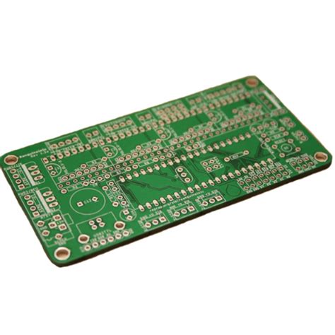
What is FR4 PCB?
FR4 (Flame Retardant 4) is a type of printed circuit board (PCB) material that is widely used in the electronics industry. It is a composite material made of woven fiberglass cloth with an epoxy resin binder. The “FR” stands for flame retardant, indicating that the material has been treated to resist ignition and slow the spread of flames in case of a fire.
FR4 PCBs are known for their excellent mechanical, electrical, and thermal properties, making them suitable for a wide range of applications. They offer good insulation, high dielectric strength, and low moisture absorption. These characteristics contribute to the reliability and durability of electronic circuits built on FR4 substrates.
Composition of FR4 PCB
The primary components of FR4 PCB material are:
- Fiberglass cloth: This is the reinforcement material that provides mechanical strength and dimensional stability to the PCB. The fiberglass is woven into a fabric and then impregnated with the epoxy resin.
- Epoxy resin: The epoxy resin acts as the binder, holding the fiberglass cloth together and providing insulation between the conductive layers. It also contributes to the PCB’s resistance to moisture, chemicals, and heat.
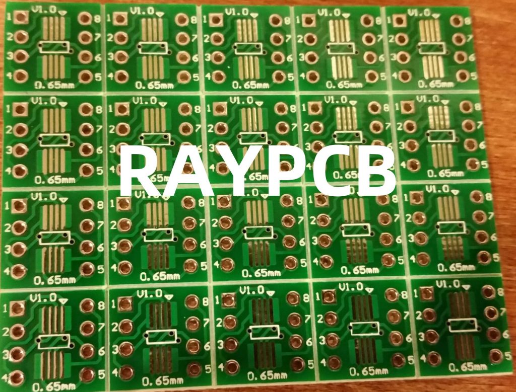
- Copper foil: Thin layers of copper foil are laminated onto one or both sides of the FR4 substrate. These copper layers are etched to create the desired circuit patterns, forming the conductive traces and pads on the PCB.
- Flame retardant additives: To enhance the fire resistance of the PCB, flame retardant chemicals are added to the epoxy resin. These additives help prevent the spread of flames and reduce the risk of fire hazards in electronic devices.
Manufacturing Process of FR4 PCB
The manufacturing process of FR4 PCBs involves several steps, each requiring precision and adherence to industry standards. Here’s an overview of the key stages:
1. PCB Design and Preparation
The first step in FR4 PCB manufacturing is designing the circuit layout using specialized software. The design includes the placement of components, routing of traces, and creation of vias and pads. Once the design is finalized, it is converted into a format suitable for manufacturing, such as Gerber files.
2. Lamination
The FR4 substrate is prepared by stacking multiple layers of pre-impregnated (prepreg) fiberglass sheets and copper foil. The number of layers depends on the complexity and requirements of the circuit. The stack is then placed in a lamination press, where high temperature and pressure are applied to bond the layers together, forming a solid and stable board.
3. Drilling
After lamination, the PCB undergoes drilling to create holes for through-hole components and vias. High-speed CNC drilling machines are used to accurately drill the holes based on the design specifications. The drilled holes are then cleaned and deburred to remove any debris.
4. Plating and Etching
The next step involves plating the drilled holes and the copper surfaces to improve conductivity and ensure proper electrical connections. A thin layer of copper is deposited onto the holes and the exposed copper areas using electroless or electrolytic plating techniques.
Once plated, the unwanted copper areas are removed through an etching process. A photoresist layer is applied to the PCB and exposed to UV light through a photomask, which selectively hardens the resist in the desired circuit pattern. The unexposed areas are then dissolved, leaving the copper traces and pads protected. The exposed copper is etched away using a chemical solution, typically ferric chloride or ammonium persulfate.
5. Solder Mask and Silkscreen
A solder mask layer is applied to the PCB to protect the copper traces and prevent solder bridges during the assembly process. The solder mask is typically green in color but can be customized based on requirements. Openings are left in the solder mask for component pads and exposed copper areas.
Silkscreen printing is then performed to add text, logos, and component identifiers to the PCB surface. The silkscreen ink is usually white but can be customized as well.
6. Surface Finish
To enhance solderability and protect the exposed copper pads from oxidation, a surface finish is applied to the PCB. Common surface finishes include:
- Hot Air Solder Leveling (HASL): A tin-lead alloy is applied to the pads and then leveled using hot air.
- Organic Solderability Preservative (OSP): A thin, organic layer is applied to the pads to prevent oxidation.
- Electroless Nickel Immersion Gold (ENIG): A layer of nickel is plated onto the pads, followed by a thin layer of gold.
7. Electrical Testing and Inspection
Before the PCBs are shipped, they undergo thorough electrical testing and visual inspection to ensure their functionality and quality. Automated optical inspection (AOI) systems are used to detect any defects or abnormalities in the PCB, such as short circuits, open circuits, or incorrect component placement.
Electrical testing is performed using specialized equipment to verify the continuity and isolation of the circuits. This helps identify any manufacturing defects or design issues that may affect the performance of the PCB.

Advantages of FR4 PCB
FR4 PCBs offer several advantages that make them a popular choice for a wide range of applications:
- Durability: FR4 material is known for its mechanical strength and stability. It can withstand high temperatures, vibrations, and impacts, making it suitable for use in harsh environments.
- Electrical insulation: The epoxy resin in FR4 provides excellent electrical insulation, preventing current leakage and ensuring reliable circuit performance.
- Flame retardancy: The flame-retardant additives in FR4 PCBs help prevent the spread of flames in case of a fire, enhancing the safety of electronic devices.
- Moisture resistance: FR4 material has low moisture absorption, which helps maintain the integrity of the PCB in humid environments.
- Cost-effectiveness: Compared to other PCB materials, FR4 offers a good balance of performance and cost, making it an economical choice for many applications.

Applications of FR4 PCB
FR4 PCBs are used in a wide variety of electronic devices and industries, including:
- Consumer electronics: FR4 is commonly used in smartphones, laptops, televisions, and home appliances.
- Automotive industry: FR4 PCBs are found in various automotive electronic systems, such as engine control units, infotainment systems, and sensors.
- Industrial equipment: Industrial control systems, power supplies, and automation devices often rely on FR4 PCBs for their reliability and durability.
- Medical devices: FR4 is used in medical equipment, such as patient monitors, diagnostic tools, and imaging systems.
- Telecommunications: FR4 PCBs are employed in routers, switches, and other networking equipment.
- Aerospace and defense: FR4 is used in avionics, radar systems, and military communication devices.
Frequently Asked Questions (FAQ)
1. What is the difference between FR4 and other PCB materials?
FR4 is a specific type of PCB material that offers a combination of good mechanical, electrical, and thermal properties. Other PCB materials, such as polyimide or high-frequency laminates, may have different characteristics suited for specific applications. FR4 is widely used due to its versatility and cost-effectiveness.
2. Can FR4 PCBs be used for high-frequency applications?
While FR4 is suitable for many general-purpose applications, it may not be the best choice for high-frequency or high-speed designs. At higher frequencies, FR4 can exhibit higher dielectric losses and signal integrity issues. For high-frequency applications, specialized materials like Rogers or Teflon-based laminates are often used.
3. What is the maximum operating temperature for FR4 PCBs?
The maximum operating temperature for FR4 PCBs depends on the specific grade and thickness of the material. Standard FR4 is rated for a continuous operating temperature of 130°C (266°F). High-temperature versions of FR4, such as FR4-HT, can withstand temperatures up to 170°C (338°F) or higher.
4. How do I choose the right thickness for my FR4 PCB?
The choice of PCB Thickness depends on various factors, such as the number of layers, component sizes, and mechanical requirements. Common thicknesses for FR4 PCBs range from 0.8mm to 3.2mm. Thicker boards provide better mechanical strength but may be more challenging to route and assemble. Consult with your PCB manufacturer to determine the optimal thickness for your specific application.
5. Are FR4 PCBs environmentally friendly?
FR4 PCBs are not inherently environmentally friendly due to the presence of flame retardants and other chemicals used in their manufacturing. However, the electronics industry has been working towards more eco-friendly solutions, such as halogen-free FR4 variants and the use of lead-free soldering processes. Proper disposal and recycling of PCBs are important to minimize their environmental impact.
Conclusion
FR4 PCB manufacturing is a complex process that involves multiple steps to create reliable and high-quality circuit boards. From the initial design and lamination to the final testing and inspection, each stage requires precision and adherence to industry standards.
FR4 PCBs offer a combination of excellent mechanical, electrical, and thermal properties, making them suitable for a wide range of applications across various industries. Their durability, flame retardancy, and cost-effectiveness have contributed to their widespread adoption in electronic devices.
As technology advances and the demand for more sophisticated electronic systems grows, FR4 PCBs continue to play a crucial role in enabling reliable and efficient circuits. By understanding the manufacturing process and characteristics of FR4 PCBs, designers and engineers can make informed decisions when selecting materials and designing circuits for their specific applications.
| PCB Material | Key Characteristics | Typical Applications |
|---|---|---|
| FR4 | – Good mechanical strength – Excellent electrical insulation – Flame retardant – Cost-effective |
– Consumer electronics – Automotive systems – Industrial equipment – Medical devices |
| Polyimide | – High temperature resistance – Flexible and bendable – Lightweight |
– Aerospace and military – Wearable electronics – High-temperature environments |
| High-Frequency Laminates | – Low dielectric loss – Stable dielectric constant – Suitable for high-speed signals |
– RF and microwave devices – Radar systems – Wireless communication equipment |
This article provides a comprehensive overview of FR4 PCB manufacturing, covering its composition, manufacturing process, advantages, applications, and frequently asked questions. By delving into the details of FR4 PCBs, readers can gain a better understanding of this essential component in the world of electronics.
No responses yet