Introduction to PCB Thickness
Printed Circuit Board (PCB) thickness is a crucial factor in the design and manufacturing of electronic devices. It plays a significant role in determining the overall performance, reliability, and durability of the final product. In this comprehensive article, we will delve into the intricacies of PCB thickness, exploring its various aspects, considerations, and best practices.
What is PCB Thickness?
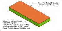
PCB thickness refers to the total thickness of the printed circuit board, including all layers of copper, substrate material, and any additional coatings or finishes. It is typically measured in mils (thousandths of an inch) or millimeters (mm). The thickness of a PCB can range from as thin as 0.4mm to as thick as 3.2mm or more, depending on the specific application and requirements.
Why is PCB Thickness Important?
PCB thickness is important for several reasons:
- Mechanical Strength: Thicker PCBs offer greater mechanical strength and rigidity, making them more resistant to bending, warping, and physical damage. This is particularly important for applications that require high reliability and durability, such as automotive, aerospace, and industrial electronics.
- Thermal Management: The thickness of a PCB can impact its thermal management properties. Thicker PCBs have better heat dissipation capabilities, allowing for more efficient cooling of components and preventing overheating. This is crucial for high-power applications or devices operating in harsh environments.
- Signal Integrity: PCB thickness can affect signal integrity, especially at high frequencies. Thinner PCBs may be more susceptible to signal loss, crosstalk, and electromagnetic interference (EMI). Proper selection of PCB thickness, along with other design considerations, helps ensure optimal signal integrity and performance.
- Manufacturing Constraints: The thickness of a PCB can influence the manufacturing process and capabilities. Thinner PCBs may require specialized equipment and techniques for fabrication and assembly, while thicker PCBs may have limitations in terms of minimum hole sizes, trace widths, and spacing.
Factors Affecting PCB Thickness Selection
When choosing the appropriate PCB thickness for a particular application, several factors need to be considered:
1. Number of Layers
The number of layers in a PCB directly impacts its thickness. Each additional layer adds to the overall thickness of the board. The number of layers required depends on the complexity of the circuit design, the number of components, and the routing requirements.
| Number of Layers | Typical Thickness Range |
|---|---|
| 1-2 Layers | 0.4mm – 1.6mm |
| 4 Layers | 0.8mm – 2.0mm |
| 6-8 Layers | 1.2mm – 2.4mm |
| 10+ Layers | 1.6mm – 3.2mm or more |
2. Copper Weight
Copper weight refers to the thickness of the copper foil used in the PCB. It is typically measured in ounces per square foot (oz/ft²). Common copper weights include 0.5oz, 1oz, 2oz, and 3oz. Thicker copper weights contribute to the overall thickness of the PCB and offer better current carrying capacity and thermal conductivity.
3. Substrate Material
The choice of substrate material also influences PCB thickness. The most common substrate materials used in PCBs are:
- FR-4: A glass-reinforced epoxy laminate, widely used for its good mechanical and electrical properties.
- High-Tg FR-4: An enhanced version of FR-4 with improved thermal stability and performance.
- Polyimide: A high-temperature, high-performance substrate material used in demanding applications.
- Aluminum: Used for metal-core PCBs (MCPCBs) to enhance thermal dissipation.
Each substrate material has its own thickness range and dielectric properties that need to be considered during the design phase.
4. Application Requirements
The specific requirements of the application play a crucial role in determining the appropriate PCB thickness. Factors such as operating environment, mechanical stress, thermal management needs, and signal integrity requirements should be carefully evaluated.
For example, automotive and aerospace applications often demand thicker PCBs for enhanced reliability and durability, while consumer electronics may prioritize thinner designs for miniaturization and weight reduction.
PCB Thickness Standards and Guidelines
To ensure consistency and compatibility in the electronics industry, various standards and guidelines have been established for PCB thickness. Some of the key standards include:
- IPC-2221: Generic Standard on Printed Board Design
- IPC-6012: Qualification and Performance Specification for Rigid Printed Boards
- IPC-4101: Specification for Base Materials for Rigid and Multilayer Printed Boards
- MIL-P-55110: Military Specification for Printed Wiring Boards
These standards provide recommendations and requirements for PCB thickness, tolerances, and other design aspects. Adhering to these standards helps ensure the manufacturability, reliability, and performance of PCBs.

PCB Thickness Measurement Techniques
Accurate measurement of PCB thickness is essential for quality control and ensuring compliance with specifications. Several techniques are commonly used for measuring PCB thickness:
- Micrometer: A manual tool that uses a spindle and anvil to measure thickness. It is suitable for quick and simple measurements but requires operator skill and may not provide the highest accuracy.
- Caliper: Another manual tool that measures thickness using a fixed jaw and a movable jaw. Calipers offer better accuracy than micrometers but still rely on operator skill.
- Thickness Gauge: An electronic device that uses a sensing probe to measure thickness. Thickness gauges provide high accuracy and repeatability and are widely used in PCB manufacturing for quality control purposes.
- Optical Measurement: Advanced optical measurement systems, such as laser micrometers or vision-based systems, can provide non-contact, high-precision thickness measurements. These systems are particularly useful for measuring thin or flexible PCBs.
PCB Thickness Tolerances and Variations
PCB thickness tolerances and variations are critical considerations in the manufacturing process. Thickness tolerances specify the acceptable range of deviation from the nominal thickness value. The tolerance requirements depend on the specific application, standards, and manufacturing capabilities.
Typical PCB thickness tolerances are:
| Thickness Range | Tolerance |
|---|---|
| < 1.0mm | ±10% |
| 1.0mm – 2.0mm | ±0.1mm |
| > 2.0mm | ±5% |
Thickness variations can occur due to several factors, including:
- Material variations: Inconsistencies in the substrate material or copper foil thickness.
- Manufacturing process variations: Differences in lamination pressure, temperature, or duration.
- Copper plating variations: Non-uniform copper plating thickness across the board.
Proper control and monitoring of the manufacturing process, along with strict adherence to quality control procedures, help minimize thickness variations and ensure consistent PCB Quality.
Best Practices for PCB Thickness Design
To optimize PCB thickness design and ensure the best performance and manufacturability, consider the following best practices:
- Collaborate with the PCB manufacturer: Engage with the PCB manufacturer early in the design process to discuss thickness requirements, tolerances, and manufacturing capabilities. Their expertise can help guide the design and avoid potential issues.
- Consider the application requirements: Carefully evaluate the specific requirements of the application, such as mechanical strength, thermal management, and signal integrity, to determine the appropriate PCB thickness.
- Follow industry standards and guidelines: Adhere to relevant industry standards and guidelines for PCB thickness and design. This ensures compatibility, reliability, and compliance with established practices.
- Optimize layer stack-up: Design the layer stack-up to achieve the desired thickness while considering signal integrity, impedance control, and manufacturability. Proper stack-up design can help minimize thickness variations and improve overall performance.
- Conduct thorough testing and validation: Perform comprehensive testing and validation of the PCB design, including thickness measurements, to ensure compliance with specifications and performance requirements. This helps identify and address any issues before mass production.
Future Trends in PCB Thickness
As technology advances and electronic devices continue to evolve, PCB thickness trends are also changing. Some of the future trends in PCB thickness include:
- Miniaturization: The demand for smaller and more compact electronic devices is driving the need for thinner PCBs. Advancements in materials, manufacturing processes, and design techniques are enabling the production of ultra-thin PCBs, often less than 0.4mm thick.
- High-Density Interconnect (HDI): HDI PCBs feature finer trace widths, smaller via sizes, and higher layer counts, allowing for increased functionality in a smaller form factor. HDI designs often require thinner PCBs to accommodate the dense interconnections and maintain signal integrity.
- Flexible and Rigid-Flex PCBs: Flexible PCBs and Rigid-flex PCBs are gaining popularity due to their ability to conform to unique shapes and withstand bending and flexing. These PCBs typically have a thinner profile compared to traditional rigid PCBs, enabling more compact and versatile designs.
- Advanced Materials: The development of advanced substrate materials, such as high-frequency laminates, low-loss dielectrics, and thermally conductive materials, is enabling the production of thinner PCBs with improved performance characteristics.
As PCB thickness continues to evolve, designers and manufacturers must stay updated with the latest technologies, materials, and processes to meet the ever-changing demands of the electronics industry.
Frequently Asked Questions (FAQ)
- What is the most common PCB thickness?
The most common PCB thickness is 1.6mm (0.063 inches). This thickness is widely used in a variety of applications and is considered a standard thickness in the industry. However, the specific thickness required may vary depending on the application and design requirements. - Can PCB thickness affect signal integrity?
Yes, PCB thickness can affect signal integrity, especially at high frequencies. Thinner PCBs may be more susceptible to signal loss, crosstalk, and electromagnetic interference (EMI). Proper selection of PCB thickness, along with other design considerations such as trace width, spacing, and dielectric material, helps ensure optimal signal integrity and performance. - How does PCB thickness impact thermal management?
PCB thickness plays a role in thermal management. Thicker PCBs have better heat dissipation capabilities due to their increased thermal mass and larger surface area for heat transfer. This allows for more efficient cooling of components and prevents overheating. In high-power applications or devices operating in harsh environments, thicker PCBs are often preferred for their enhanced thermal management properties. - What are the challenges associated with thin PCBs?
Thin PCBs, typically less than 0.8mm thick, pose several challenges in terms of design, manufacturing, and handling. Some of the challenges include: - Increased fragility and susceptibility to damage during handling and assembly.
- Difficulty in achieving reliable soldered joints due to limited heat capacity.
- Potential signal integrity issues, such as increased crosstalk and impedance variations.
- Limited space for routing traces and placing components.
- Specialized manufacturing processes and equipment requirements.
Designers and manufacturers must carefully consider these challenges and implement appropriate measures to ensure the reliability and performance of thin PCBs.
- How can I ensure consistent PCB thickness in my design?
To ensure consistent PCB thickness in your design, consider the following: - Collaborate closely with your PCB manufacturer and communicate your thickness requirements clearly.
- Adhere to industry standards and guidelines for PCB thickness and tolerances.
- Optimize your layer stack-up design to achieve the desired thickness while maintaining signal integrity and manufacturability.
- Specify appropriate thickness tolerances and work with your manufacturer to establish quality control measures.
- Conduct thorough testing and measurement of PCB thickness during prototyping and production to identify and address any variations.
By following these practices and maintaining open communication with your PCB manufacturer, you can minimize thickness variations and ensure consistent PCB quality.
Conclusion
PCB thickness is a critical aspect of PCB design and manufacturing, influencing the performance, reliability, and manufacturability of electronic devices. Understanding the factors that affect PCB thickness, such as the number of layers, copper weight, substrate material, and application requirements, is essential for making informed design decisions.
Adhering to industry standards, collaborating with PCB manufacturers, and following best practices for PCB thickness design can help optimize the performance and reliability of PCBs while meeting the specific needs of the application.
As technology advances and the demand for smaller, high-performance electronic devices grows, PCB thickness will continue to evolve. Designers and manufacturers must stay updated with the latest trends, materials, and processes to meet the challenges and opportunities presented by PCB thickness in the ever-changing landscape of the electronics industry.
No responses yet