Introduction to Reflow Soldering
Reflow soldering is a crucial process in the assembly of printed circuit boards (PCBs) that involves melting solder paste to create permanent electrical connections between surface mount components and the PCB. This technique is widely used in the electronics manufacturing industry due to its efficiency, reliability, and ability to handle high-volume production. In this article, we will explore the fundamentals of reflow soldering, its advantages, and the various stages involved in the process.
What is Reflow Soldering?
Reflow soldering is a process that uses heat to melt solder paste, which is a mixture of tiny solder particles suspended in flux. The molten solder then forms a strong bond between the leads of surface mount components and the pads on the PCB. This process is typically carried out in a reflow oven, which precisely controls the temperature profile to ensure optimal soldering results.
Advantages of Reflow Soldering
- High efficiency: Reflow soldering allows for the simultaneous soldering of multiple components, significantly reducing the time required for PCB Assembly.
- Consistency: The controlled temperature profile in a reflow oven ensures consistent and reliable solder joints across the entire PCB.
- Miniaturization: Reflow soldering enables the use of smaller components and fine-pitch leads, facilitating the production of compact and high-density PCBs.
- Automated process: Reflow soldering can be easily automated, minimizing human error and increasing overall production efficiency.
The Reflow Soldering Process
The reflow soldering process consists of several stages, each playing a critical role in achieving high-quality solder joints. Let’s take a closer look at each stage:
1. Solder Paste Application
The first step in the reflow soldering process is applying solder paste to the PCB. This is typically done using a stencil printing method, where a thin metal stencil with openings corresponding to the pads on the PCB is placed over the board. Solder paste is then spread across the stencil, filling the openings and depositing the paste onto the pads.
Stencil Design Considerations
- Aperture size: The openings in the stencil should be slightly larger than the pads on the PCB to ensure adequate solder paste coverage.
- Stencil thickness: The thickness of the stencil determines the amount of solder paste deposited. Thicker stencils result in more solder paste, which is suitable for larger components or high-thermal-mass pads.
- Stencil material: Stainless steel is the most common material used for solder paste stencils due to its durability and precision.
2. Component Placement
After applying the solder paste, surface mount components are placed onto the PCB using a pick-and-place machine or by hand. The components are positioned according to their designated locations on the PCB Layout, with their leads aligned with the solder paste deposits on the pads.
Factors Affecting Component Placement Accuracy
- Machine calibration: Pick-and-place machines must be properly calibrated to ensure precise component placement.
- Component packaging: The type of packaging, such as tape and reel, trays, or tubes, can affect the placement accuracy and efficiency.
- Fiducial Markers: Fiducial markers on the PCB help the pick-and-place machine align the board and components accurately.
3. Reflow Soldering Profile
The reflow soldering profile is a critical aspect of the process, as it determines the time and temperature exposure of the PCB and components during soldering. A typical reflow profile consists of four main stages:
- Preheat: The PCB is gradually heated to evaporate the solvents in the solder paste and activate the flux.
- Thermal soak: The temperature is maintained just below the melting point of the solder to ensure even heat distribution across the PCB and components.
- Reflow: The temperature is rapidly increased above the melting point of the solder, causing the solder particles to melt and form a strong bond between the components and the PCB.
- Cooling: The PCB is cooled down to solidify the solder joints and prevent thermal shock to the components.
| Stage | Temperature Range | Duration |
|---|---|---|
| Preheat | 150°C – 180°C | 60-90 sec |
| Thermal Soak | 180°C – 200°C | 60-120 sec |
| Reflow | 220°C – 250°C | 30-60 sec |
| Cooling | < 100°C | 30-60 sec |
Note: The temperature ranges and durations provided in the table are general guidelines and may vary depending on the specific solder paste and components used.
Factors Influencing the Reflow Profile
- Solder paste: Different solder pastes have varying melting points and flux activation temperatures, which affect the reflow profile.
- Component thermal mass: Larger components with higher thermal mass require more time and energy to reach the desired temperature.
- PCB design: The layout and density of the PCB can impact the heat distribution and, consequently, the reflow profile.
4. Inspection and Quality Control
After the reflow soldering process is complete, the PCB undergoes inspection and quality control to ensure the integrity of the solder joints and the overall functionality of the board. Several methods are used for this purpose:
- Visual inspection: A trained operator visually examines the solder joints for defects such as bridging, Insufficient Solder, or poor wetting.
- Automated optical inspection (AOI): An AOI machine uses high-resolution cameras and image processing algorithms to detect soldering defects automatically.
- X-ray inspection: For PCBs with hidden or obscured solder joints, such as those found in Ball Grid Array (BGA) packages, X-ray inspection is used to verify the quality of the connections.
- Electrical testing: Functional tests are performed to ensure that the PCB operates as intended and meets the specified performance criteria.

Common Reflow Soldering Defects and Their Causes
Despite the controlled nature of the reflow soldering process, various defects can occur due to factors such as improper solder paste application, incorrect component placement, or suboptimal reflow profile. Some common defects include:
- Bridging: Excess solder forming a connection between adjacent pads or leads.
-
Causes: Overprinting of solder paste, incorrect stencil design, or component misalignment.
-
Insufficient solder: Incomplete or weak solder joints due to inadequate solder paste coverage.
-
Causes: Underprinting of solder paste, incorrect stencil design, or poor wetting of the solder.
-
Tombstoning: One end of a component lifting off the PCB during reflow, resulting in a vertical standing component.
-
Causes: Uneven heating, component misalignment, or imbalanced solder paste deposits.
-
Solder balls: Small spheres of solder that form on the PCB surface or component leads.
- Causes: Excessive solder paste, contamination, or incorrect reflow profile.
To minimize the occurrence of these defects, it is essential to optimize the reflow soldering process, including proper solder paste application, accurate component placement, and a well-designed reflow profile.

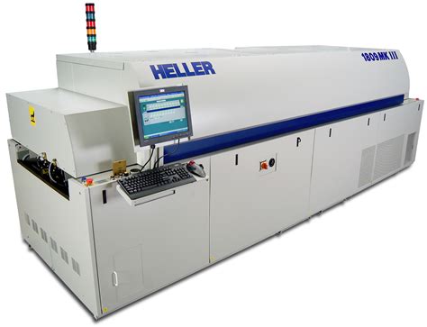
Selecting the Right Reflow Soldering Equipment
Choosing the appropriate reflow soldering equipment is crucial for achieving consistent and high-quality results. When selecting a reflow oven, consider the following factors:
- Oven type: Reflow ovens can be convection-based, infrared (IR), or vapor phase. Each type has its advantages and limitations, and the choice depends on the specific requirements of the PCB assembly process.
- Temperature control: The reflow oven should have precise temperature control and the ability to maintain a stable temperature profile throughout the soldering process.
- Oven size: The size of the reflow oven should accommodate the dimensions of the PCBs being assembled and the expected production volume.
- Nitrogen atmosphere: Some reflow ovens offer the option of a nitrogen atmosphere, which can help reduce oxidation and improve solder joint quality.
- Cooling system: An efficient cooling system is essential to prevent thermal shock to the components and ensure proper solidification of the solder joints.

Best Practices for Reflow Soldering
To optimize the reflow soldering process and achieve the best possible results, consider the following best practices:
- Use high-quality solder paste: Select a solder paste with the appropriate alloy composition, particle size, and flux activity for your specific application.
- Maintain proper storage and handling of solder paste: Solder paste should be stored at the recommended temperature and used within its shelf life to ensure optimal performance.
- Implement a robust stencil printing process: Regularly clean and inspect the stencil, and optimize the printing parameters, such as pressure, speed, and separation distance.
- Ensure accurate component placement: Regularly calibrate the pick-and-place machine and use appropriate component packaging to maintain placement accuracy.
- Develop and optimize the reflow profile: Create a reflow profile tailored to the specific solder paste and components used, and regularly monitor and adjust the profile as needed.
- Conduct thorough inspection and quality control: Implement a combination of visual, automated, and electrical testing methods to identify and address any soldering defects promptly.
By following these best practices and continuously monitoring and improving the reflow soldering process, manufacturers can ensure the production of high-quality, reliable PCBs.
Frequently Asked Questions (FAQ)
- What is the difference between reflow soldering and wave soldering?
-
Reflow soldering is used for surface mount components and involves melting solder paste to create connections between the components and the PCB. Wave soldering, on the other hand, is used for through-hole components and involves passing the PCB over a molten solder wave to create solder joints.
-
Can reflow soldering be used for through-hole components?
-
While reflow soldering is primarily used for surface mount components, it can be used for certain through-hole components with suitable leads and thermal characteristics. However, wave soldering is generally more suitable for through-hole components.
-
What is the purpose of flux in solder paste?
-
Flux serves several purposes in solder paste, including removing oxides from the metal surfaces, preventing reoxidation during soldering, and promoting the wetting and spreading of the molten solder to create a strong bond between the components and the PCB.
-
How can I troubleshoot a reflow soldering process that produces defects?
-
To troubleshoot a reflow soldering process, first identify the specific defects occurring. Then, systematically review and optimize each stage of the process, including solder paste application, component placement, and the reflow profile. Conduct thorough inspections and make incremental adjustments until the defects are minimized or eliminated.
-
What safety precautions should be taken when working with reflow soldering equipment?
- When working with reflow soldering equipment, always wear appropriate personal protective equipment (PPE), such as heat-resistant gloves and safety glasses. Ensure proper ventilation to minimize exposure to fumes and vapors, and follow the manufacturer’s guidelines for safe operation and maintenance of the equipment.
Conclusion
Reflow soldering is a critical process in the assembly of printed circuit boards, enabling the efficient and reliable creation of electrical connections between surface mount components and the PCB. By understanding the fundamentals of reflow soldering, including the various stages and factors that influence the process, manufacturers can optimize their PCB assembly lines to produce high-quality, defect-free boards.
Implementing best practices, such as using high-quality solder paste, maintaining accurate component placement, and developing a well-designed reflow profile, is essential for achieving consistent and reliable results. Additionally, regular inspection and quality control measures help identify and address any soldering defects promptly, ensuring the production of PCBs that meet the required performance and reliability standards.
As the electronics industry continues to evolve, with the increasing miniaturization of components and the demand for high-density PCBs, the importance of a well-controlled and optimized reflow soldering process will only continue to grow. By staying informed about the latest developments in reflow soldering technology and best practices, manufacturers can remain competitive and deliver innovative, high-quality electronic products to their customers.
No responses yet