
Introduction to Electronics Manufacturing
Electronics manufacturing is the process of designing, developing, testing, and producing electronic components, devices, and systems. It involves a wide range of activities, from the production of individual components to the assembly of complex electronic systems. The electronics manufacturing industry has seen significant growth in recent years, driven by the increasing demand for electronic devices in various sectors, including consumer electronics, automotive, aerospace, and healthcare.
Key Aspects of Electronics Manufacturing
- Design and Development
- Component Manufacturing
- PCB Fabrication
- Assembly and Integration
- Testing and Quality Control
Design and Development in Electronics Manufacturing
The design and development phase is crucial in electronics manufacturing. It involves the creation of electronic circuits, components, and systems that meet specific requirements and functionalities. This phase typically includes the following steps:
Steps in Design and Development
- Concept Development
- Schematic Design
- PCB Layout Design
- Prototyping and Testing
- Design Validation and Optimization
Concept Development
In the concept development stage, engineers and designers collaborate to define the specifications and requirements of the electronic device or system. They consider factors such as functionality, performance, size, power consumption, and cost.
Schematic Design
Once the concept is developed, engineers create a schematic diagram that represents the electronic circuit. The schematic shows the interconnections between components and provides a visual representation of the circuit’s functionality.
PCB Layout Design
After the schematic design is complete, the next step is to create a PCB (Printed Circuit Board) layout. The PCB layout determines the physical placement of components and the routing of traces that connect them. PCB design software is used to create the layout, ensuring optimal component placement and signal integrity.
Prototyping and Testing
With the PCB layout complete, a prototype is fabricated for testing and validation. The prototype is subjected to various tests to ensure that it meets the desired specifications and functions as intended. Any issues or defects identified during testing are addressed and corrected.
Design Validation and Optimization
After successful prototyping and testing, the design undergoes a final validation process. This involves reviewing the design for manufacturability, reliability, and compliance with industry standards. Any necessary optimizations are made to improve the design’s performance, cost-effectiveness, and manufacturability.
Component Manufacturing in Electronics Manufacturing
Component manufacturing is a critical aspect of electronics manufacturing. It involves the production of individual electronic components that are used in the assembly of electronic devices and systems. Some common components manufactured in the electronics industry include:
Common Electronic Components
- Resistors
- Capacitors
- Inductors
- Diodes
- Transistors
- Integrated Circuits (ICs)
Resistors
Resistors are passive components that oppose the flow of electric current in a circuit. They are used to control voltage levels, limit current, and provide specific resistance values. Resistors are manufactured using various materials, such as carbon, metal film, and wire-wound, depending on the required specifications.
Capacitors
Capacitors are passive components that store electrical energy in an electric field. They are used for filtering, coupling, and decoupling in electronic circuits. Capacitors come in different types, such as ceramic, electrolytic, and tantalum, each with specific characteristics and applications.
Inductors
Inductors are passive components that store energy in a magnetic field when electric current flows through them. They are used in various applications, such as power supplies, filters, and oscillators. Inductors can be manufactured using different core materials, such as air, ferrite, and iron, depending on the desired properties.
Diodes
Diodes are semiconductor components that allow current to flow in only one direction. They are used for rectification, protection, and switching in electronic circuits. Common types of diodes include PN junction diodes, Schottky diodes, and Zener diodes.
Transistors
Transistors are semiconductor devices that can amplify or switch electronic signals. They are the building blocks of modern electronics and are used in a wide range of applications, from simple circuits to complex integrated circuits. Transistors come in different types, such as bipolar junction transistors (BJTs) and field-effect transistors (FETs).
Integrated Circuits (ICs)
Integrated circuits are miniaturized electronic circuits that combine multiple components, such as transistors, diodes, and resistors, on a single semiconductor chip. ICs are used in virtually all electronic devices, from smartphones and computers to automotive and industrial systems. They offer high functionality, reliability, and miniaturization.

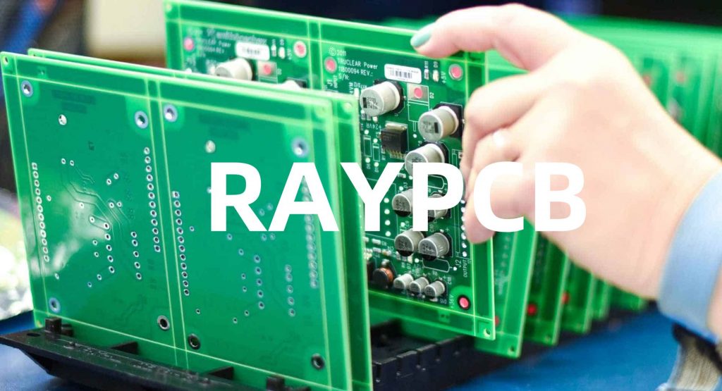
PCB Fabrication in Electronics Manufacturing
PCB (Printed Circuit Board) fabrication is a crucial step in electronics manufacturing. It involves the production of the physical board that holds and connects the electronic components. The PCB fabrication process typically includes the following steps:
PCB Fabrication Process
- Material Selection
- Copper Clad Lamination
- Drilling
- Copper Patterning
- Solder Mask Application
- Silkscreen Printing
- Surface Finish Application
Material Selection
The first step in PCB fabrication is selecting the appropriate substrate material. The most common substrate material is FR-4, a glass-reinforced epoxy laminate. Other materials, such as polyimide or PTFE, may be used for specific applications that require high temperature resistance or low dielectric constant.
Copper Clad Lamination
The selected substrate material is laminated with a thin layer of copper on one or both sides. The copper layer serves as the conductive material for the circuit traces. The lamination process involves applying heat and pressure to bond the copper to the substrate.
Drilling
Holes are drilled through the PCB to accommodate through-hole components and provide interconnections between layers. The drilling process is performed using computer-controlled drill machines that ensure precise hole placement and size.
Copper Patterning
The desired copper pattern, which represents the circuit traces, is created on the PCB. This is typically done using a photolithography process. A photoresist layer is applied to the copper surface, and the circuit pattern is transferred to the photoresist using a photomask and UV light exposure. The exposed photoresist is then developed, and the unwanted copper is etched away, leaving the desired copper pattern.
Solder Mask Application
A solder mask, usually green in color, is applied to the PCB surface. The solder mask covers the copper traces, leaving only the exposed pads and areas where components will be soldered. The solder mask provides insulation, protection, and improves the solderability of the PCB.
Silkscreen Printing
A silkscreen layer is printed on the PCB surface to add text, logos, and component identifiers. The silkscreen is usually white and helps in the assembly process by providing visual references for component placement.
Surface Finish Application
A surface finish is applied to the exposed copper pads to protect them from oxidation and enhance solderability. Common surface finishes include HASL (Hot Air Solder Leveling), ENIG (Electroless Nickel Immersion Gold), and OSP (Organic Solderability Preservative).
Assembly and Integration in Electronics Manufacturing
Assembly and integration are the processes of placing and connecting electronic components on the fabricated PCB to create a functional electronic device or system. This stage involves several steps, including:
Assembly and Integration Steps
- Solder Paste Printing
- Component Placement
- Soldering
- Inspection and Testing
- Final Assembly and Packaging
Solder Paste Printing
Solder paste, a mixture of tiny solder particles and flux, is printed onto the PCB pads using a stencil. The stencil ensures precise application of the solder paste, which is essential for proper component attachment.
Component Placement
Electronic components are placed onto the PCB using automated pick-and-place machines. These machines accurately position the components on the solder paste-printed pads. Surface mount devices (SMDs) are the most common type of components used in modern electronics manufacturing.
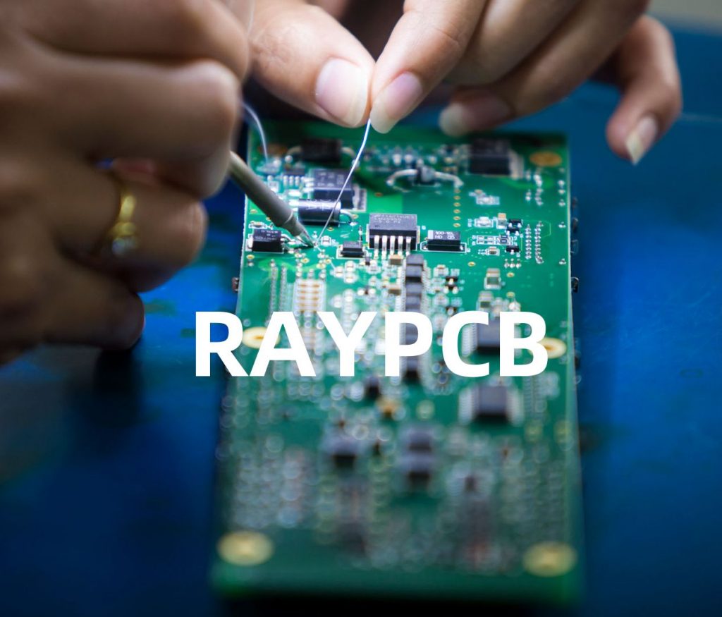
Soldering
The PCB with placed components undergoes a soldering process to establish electrical connections. The most common soldering method is reflow soldering, where the PCB is passed through a reflow oven. The oven applies a controlled temperature profile, melting the solder paste and forming a strong bond between the components and the PCB pads.
Inspection and Testing
After soldering, the assembled PCB undergoes inspection and testing to ensure the quality and functionality of the electronic device. Automated optical inspection (AOI) systems are used to detect any soldering defects or component placement issues. Electrical testing, such as in-circuit testing (ICT) or functional testing, is performed to verify the device’s performance and functionality.
Final Assembly and Packaging
Once the assembled PCB has passed the inspection and testing stages, it undergoes final assembly and packaging. This may involve incorporating the PCB into a housing or enclosure, adding user interfaces (e.g., displays, buttons), and connecting power sources or other modules. The final product is then packaged and prepared for distribution.
Testing and Quality Control in Electronics Manufacturing
Testing and quality control are essential aspects of electronics manufacturing. They ensure that the manufactured products meet the required specifications, performance standards, and reliability expectations. Various types of tests are conducted at different stages of the manufacturing process, including:
Types of Testing
- In-Circuit Testing (ICT)
- Functional Testing
- Burn-In Testing
- Environmental Testing
- Reliability Testing
In-Circuit Testing (ICT)
In-circuit testing is performed to verify the correctness of the PCB Assembly. It involves using a bed-of-nails fixture that makes contact with specific test points on the PCB. The test system applies electrical signals and measures the responses to detect any short circuits, open circuits, or component failures.
Functional Testing
Functional testing is conducted to validate the overall functionality and performance of the electronic device. It involves subjecting the device to various operational scenarios and verifying that it functions as intended. Functional testing may include tests for power consumption, signal integrity, and communication interfaces.
Burn-In Testing
Burn-in testing is a type of stress testing that involves operating the electronic device under elevated temperature and voltage conditions for an extended period. The purpose of burn-in testing is to identify and eliminate early-life failures and ensure the long-term reliability of the device.
Environmental Testing
Environmental testing assesses the electronic device’s ability to withstand various environmental conditions, such as temperature extremes, humidity, vibration, and shock. These tests simulate the real-world operating conditions that the device may encounter during its lifecycle.
Reliability Testing
Reliability testing is conducted to evaluate the long-term durability and performance of the electronic device. It involves subjecting the device to accelerated life testing, where it is exposed to stress factors (e.g., temperature cycling, power cycling) to estimate its expected lifespan and failure rates.
Conclusion
Electronics manufacturing is a complex and multifaceted process that involves various stages, from design and development to component manufacturing, PCB fabrication, assembly, and testing. Each stage plays a crucial role in ensuring the quality, reliability, and functionality of the final electronic product.
As the demand for electronic devices continues to grow across industries, electronics manufacturers must continuously innovate and adapt to new technologies, materials, and manufacturing processes. By implementing robust quality control measures, leveraging automation, and staying updated with the latest industry trends, electronics manufacturers can deliver high-quality products that meet the evolving needs of their customers.
Frequently Asked Questions (FAQ)
- What is the difference between through-hole and surface mount components?
Through-hole components have leads that are inserted into holes drilled in the PCB and soldered on the opposite side. Surface mount components are placed directly on the PCB pads and soldered using reflow soldering. Surface mount technology allows for smaller component sizes and higher component density on the PCB. - What is the purpose of a solder mask on a PCB?
A solder mask is a protective layer applied to the PCB surface that covers the copper traces, leaving only the exposed pads and areas where components will be soldered. The solder mask provides insulation, protection against short circuits, and improves the solderability of the PCB by preventing solder bridges between closely spaced pads. - What is the difference between reflow soldering and wave soldering?
Reflow soldering is used for surface mount components and involves printing solder paste on the PCB pads, placing components, and passing the PCB through a reflow oven to melt the solder and form connections. Wave soldering is used for through-hole components and involves passing the PCB over a molten solder wave, which fills the through-holes and creates solder joints. - What is the purpose of burn-in testing in electronics manufacturing?
Burn-in testing is a type of stress testing that involves operating the electronic device under elevated temperature and voltage conditions for an extended period. The purpose of burn-in testing is to identify and eliminate early-life failures, also known as infant mortality failures, and ensure the long-term reliability of the device. - What are some common surface finishes used in PCB fabrication?
Common surface finishes used in PCB fabrication include: - HASL (Hot Air Solder Leveling): A tin-lead alloy is applied to the exposed copper pads using a hot air leveling process.
- ENIG (Electroless Nickel Immersion Gold): A layer of nickel is deposited on the copper pads, followed by a thin layer of gold to prevent oxidation.
- OSP (Organic Solderability Preservative): A thin, organic coating is applied to the copper pads to prevent oxidation and enhance solderability.
- Immersion Silver: A thin layer of silver is deposited on the copper pads to provide good solderability and electrical conductivity.
No responses yet