
Step 1: Choose the Right PCB Design Software
Choosing the right PCB design software is crucial to the success of your project. There are many options available, ranging from free open-source software to expensive commercial programs. Some popular options include:
| Software | Description | Price |
|---|---|---|
| KiCad | Open-source PCB design software | Free |
| Eagle | Popular PCB design software with a free version | Free for non-commercial use |
| Altium Designer | High-end PCB design software for professionals | $$$$ |
When choosing PCB design software, consider your budget, experience level, and the complexity of your project. If you’re just starting out, a free option like KiCad or the free version of Eagle may be sufficient. As you gain more experience and take on more complex projects, you may want to invest in a more powerful tool like Altium Designer.
Step 2: Create a Schematic Diagram
Before you start designing your PCB, you need to create a schematic diagram. A schematic diagram is a visual representation of your circuit, showing all the components and how they are connected. This step is crucial because it helps you identify any design flaws or potential issues before you start laying out your PCB.
When creating your schematic diagram, be sure to:
- Use standard symbols for components
- Label all components and pins clearly
- Use a consistent naming convention for nets and signals
- Double-check all connections and pinouts
Step 3: Choose the Right Components
Choosing the right components for your PCB Prototype is essential to its success. When selecting components, consider factors such as:
- Cost
- Availability
- Performance
- Size
- Compatibility with your design
To keep costs low, look for components that are readily available and inexpensive. You may also want to consider using surface-mount components, which are smaller and cheaper than through-hole components.

Step 4: Design Your PCB Layout
Once you have your schematic diagram and components selected, it’s time to start designing your PCB layout. This is where you’ll determine the physical placement of components on the board and route the traces that connect them.
When designing your PCB layout, keep the following tips in mind:
- Keep trace lengths as short as possible to minimize signal loss and interference
- Use a grid to keep components aligned and spaced evenly
- Avoid sharp angles in traces, which can cause signal reflections
- Use ground planes to reduce noise and improve signal integrity
- Keep high-speed signals away from sensitive analog circuits
- Use copper pours to improve heat dissipation and reduce EMI
Step 5: Choose the Right PCB Manufacturer
Choosing the right PCB manufacturer is critical to the success of your prototype. When selecting a manufacturer, consider factors such as:
- Cost
- Turnaround time
- Quality
- Minimum order quantity
- Customer service
To keep costs low, look for PCB manufacturers that offer low minimum order quantities and competitive pricing. Some popular low-cost PCB manufacturers include:
| Manufacturer | Minimum Order Quantity | Lead Time | Price |
|---|---|---|---|
| JLCPCB | 5 | 24 hours | $ |
| PCBWay | 5 | 24 hours | $ |
| OSH Park | 3 | 12 days | $$ |
| Seeed Studio | 5 | 7 days | $ |
Step 6: Generate Gerber Files
Once your PCB layout is complete, you need to generate Gerber files. Gerber files are the standard format used by PCB manufacturers to fabricate your board. Most PCB design software includes tools for generating Gerber files.
When generating Gerber files, be sure to:
- Include all necessary layers (top copper, bottom copper, silkscreen, solder mask, etc.)
- Use the correct file extensions for each layer
- Include a drill file for any through-hole components
- Double-check the Gerber files for errors or missing features
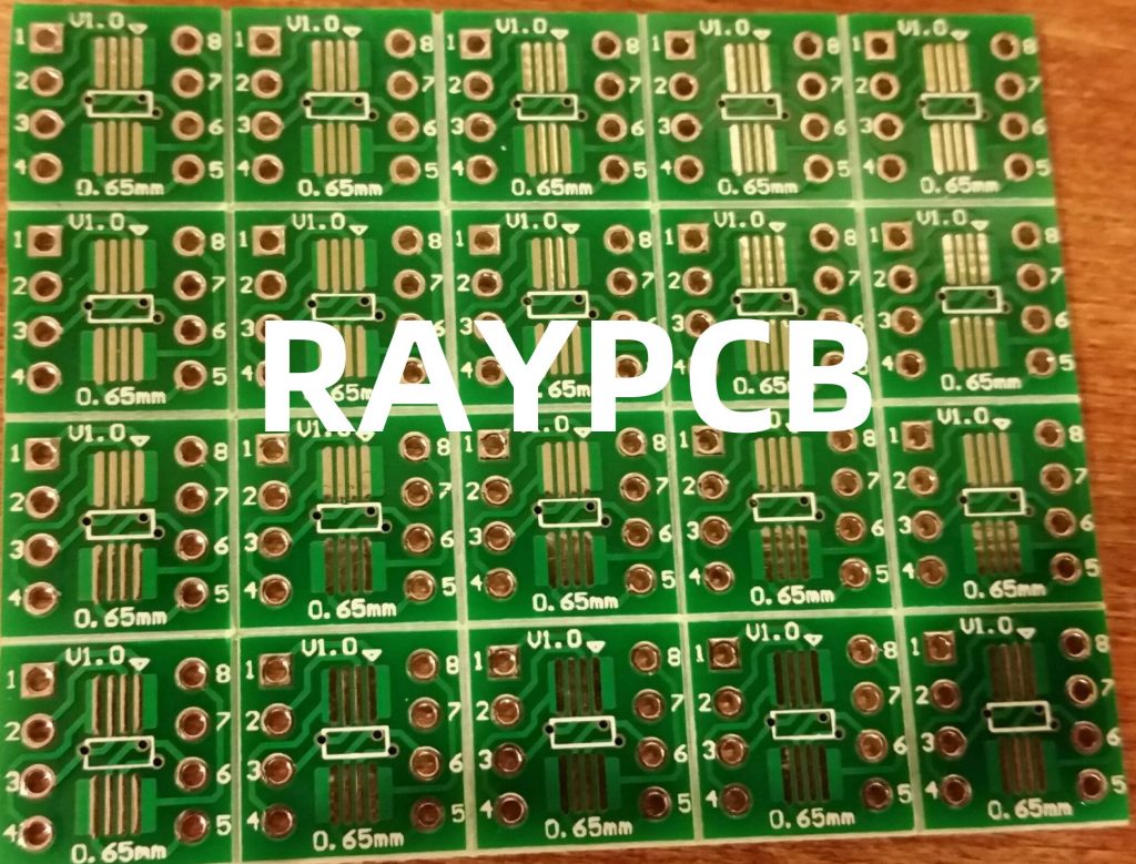
Step 7: Order Your PCB Prototypes
With your Gerber files generated, you’re ready to order your PCB prototypes. Most PCB manufacturers have an online ordering process that allows you to upload your Gerber files, select your desired specifications, and place your order.
When ordering your PCB prototypes, be sure to:
- Double-check your Gerber files for errors
- Select the correct PCB thickness, copper weight, and solder mask color
- Choose a suitable surface finish (HASL, ENIG, OSP, etc.)
- Specify any special requirements such as Castellated Holes or Gold Fingers
- Review your order carefully before submitting
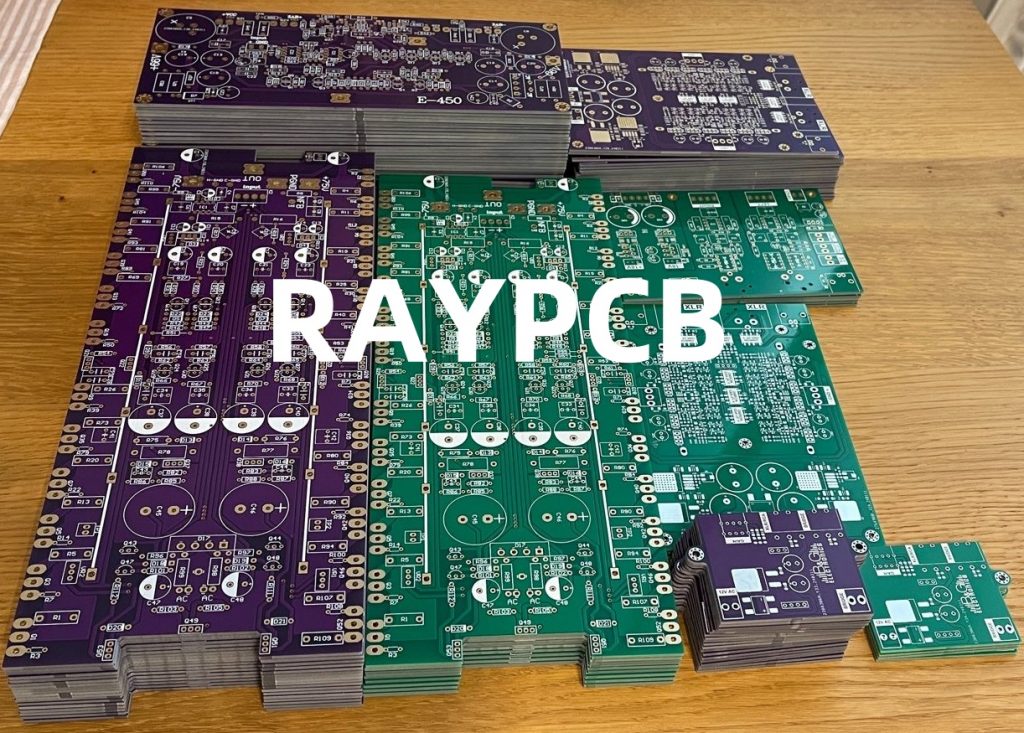
Step 8: Assemble Your PCB Prototypes
Once you receive your PCB prototypes from the manufacturer, it’s time to assemble them. If you’re comfortable with soldering, you can assemble the boards yourself. If not, you may want to consider using an assembly service.
When assembling your PCB prototypes, keep the following tips in mind:
- Use a clean, well-lit workspace
- Wear eye protection and use proper ventilation when soldering
- Use a good quality soldering iron and solder
- Start with the smallest components and work your way up to larger ones
- Double-check component placement and orientation before soldering
- Use flux to improve solder joint quality and prevent bridging
- Clean the board thoroughly after soldering to remove flux residue
Step 9: Test Your PCB Prototypes
After assembling your PCB prototypes, it’s important to test them thoroughly to ensure they function as intended. Testing can help you identify any design flaws, assembly errors, or component failures.
When testing your PCB prototypes, consider the following:
- Use a multimeter to check for short circuits and open connections
- Use an oscilloscope to verify signal integrity and timing
- Test all functions and features of the board
- Stress test the board under different conditions (temperature, humidity, vibration, etc.)
- Keep detailed records of your test results for future reference
Step 10: Iterate and Refine Your Design
Based on the results of your testing, you may need to iterate and refine your design. This may involve making changes to your schematic diagram, PCB layout, or component selection.
When iterating on your design, keep the following tips in mind:
- Focus on fixing the most critical issues first
- Use simulation tools to verify changes before committing to a new prototype
- Keep detailed notes on each iteration of your design
- Consider seeking feedback from other engineers or experts in your field
Step 11: Optimize for Manufacturing
Once you have a functional prototype that meets your requirements, it’s time to optimize your design for manufacturing. This involves making changes to your design to improve its manufacturability, reliability, and cost-effectiveness.
When optimizing for manufacturing, consider the following:
- Use standard component sizes and packages wherever possible
- Avoid using components that are difficult to source or have long lead times
- Use design for manufacturing (DFM) techniques to improve yields and reduce costs
- Consider using automated assembly processes such as pick-and-place machines
- Work closely with your PCB manufacturer to ensure your design is optimized for their processes
Step 12: Create a Bill of Materials (BOM)
A bill of materials (BOM) is a comprehensive list of all the components used in your PCB design. It includes information such as part numbers, quantities, and suppliers.
When creating your BOM, be sure to:
- Use a consistent format and naming convention
- Include all necessary information (part number, description, quantity, supplier, etc.)
- Double-check the BOM against your schematic diagram and PCB layout
- Consider using a spreadsheet or BOM management tool to keep track of changes
Step 13: Document Your Design
Proper documentation is essential for any PCB design project. It helps ensure that your design can be easily understood, maintained, and modified by others.
When documenting your design, be sure to include:
- A detailed schematic diagram
- A PCB layout file
- A bill of materials (BOM)
- Assembly instructions and guidelines
- Test procedures and results
- Any relevant datasheets, application notes, or reference designs
Step 14: Plan for the Future
Finally, it’s important to plan for the future of your PCB design. This may involve considering factors such as:
- Scalability – Can your design be easily scaled up for mass production?
- Upgradability – Can your design be easily upgraded or modified to meet changing requirements?
- Obsolescence – Are any of the components used in your design at risk of becoming obsolete?
- Intellectual property – Have you properly protected your design and any proprietary technology?
By planning for the future, you can ensure that your PCB design remains viable and competitive in the long term.
Frequently Asked Questions (FAQ)
- What is a PCB prototype?
- A PCB prototype is an early version of a printed circuit board that is used for testing and validation. It allows designers to verify the functionality and performance of their design before committing to a full production run.
- How much does it cost to build a PCB prototype?
- The cost of building a PCB prototype varies depending on factors such as the size and complexity of the board, the number of layers, and the components used. However, by following the steps outlined in this article, it is possible to build a PCB prototype at a relatively low cost, typically ranging from $10 to $100 per board.
- What software is used for PCB design?
- There are many software options available for PCB design, ranging from free open-source programs like KiCad to expensive commercial tools like Altium Designer. The choice of software depends on factors such as budget, experience level, and the complexity of the project.
- How long does it take to build a PCB prototype?
- The time required to build a PCB prototype depends on several factors, including the complexity of the design, the availability of components, and the turnaround time of the PCB manufacturer. In general, it can take anywhere from a few days to several weeks to go from initial design to a fully assembled and tested prototype.
- What are some common mistakes to avoid when building a PCB prototype?
- Some common mistakes to avoid when building a PCB prototype include:
- Using the wrong component values or footprints
- Failing to properly ground the board or use appropriate shielding
- Not thoroughly testing the prototype before moving to production
- Not documenting the design properly or creating a complete bill of materials
- Not considering manufacturability or scalability when designing the board
By avoiding these mistakes and following the steps outlined in this article, you can increase your chances of success when building a PCB prototype at low cost.
No responses yet