The Evolution of Printed Circuit Boards
Early Origins of PCBs in the 20th Century
The printed circuit board (PCB) has revolutionized electronics since its invention in the early 20th century. The concept originated in 1903 when German inventor Albert Hanson filed a patent for creating an electrical connection on an insulated surface by printing through a stencil with conductive ink. However, it wasn’t until the 1920s that Charles Ducas of the United States created circuits in an additive process of electroplating Copper Foil patterns onto an insulated substrate.
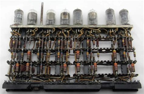
In the 1930s and 1940s, PCBs started being used more widely, especially in military applications during World War II. The inventor Paul Eisler, working in the UK, made further advances by etching away unwanted metal to leave behind copper tracks on an insulating board. His techniques formed the basis of modern PCB manufacturing.
| Decade | PCB Development Milestones |
|---|---|
| 1900s | Albert Hanson patents conductive ink printing through stencil |
| 1920s | Charles Ducas creates additive process circuits on insulated substrate |
| 1930s-40s | Paul Eisler develops etching techniques, PCBs used in military equipment in WWII |
PCB Advances in the 1950s-1970s
After the war, the PCB industry began to grow rapidly as the technology was adopted for commercial electronics. Developments in materials and manufacturing techniques enabled the production of double-sided PCBs with plated through-holes connecting circuits on both sides of the board.
In the 1950s, solder mask coatings were introduced to prevent solder bridging. Silk screen printing of component designators also became common. Companies like Hazeltyne and Motorola mass produced PCBs for commercial electronics and early computers.
The 1960s saw the rise of multilayer PCBs, allowing for even greater circuit density. IBM, Lear, and others filed early patents for Multilayer PCB Manufacturing. Photosensitive materials began to be used for creating etch-resistant traces for more precise control.
By the 1970s, PCBs were ubiquitous in electronics. Flexible circuits and surface mount technologies emerged. Computer-aided manufacturing became increasingly important for PCB design and production as devices grew more complex.
| Decade | PCB Advances |
|---|---|
| 1950s | Double-sided boards, plated through-holes, solder mask, silk screen component labels |
| 1960s | Multilayer boards, photosensitive etch-resists |
| 1970s | Flexible circuits, surface mount technology, computer-aided design and manufacturing |
PCBs from the 1980s to Today
Since the 1980s, PCBs have become increasingly sophisticated with advances in materials, design, and manufacturing. Some key developments include:
- High density interconnect (HDI) PCBs with microvias and embedded components
- Fine pitch BGAs and chip scale packages
- Controlled impedance for high frequency RF/microwave designs
- Heavy copper boards for high current applications
- Rigid-Flex PCBs combining rigid and flexible circuit sections
- Environmentally-friendly lead-free processing and halogen-free materials
Specialized PCB materials have been engineered for different applications, such as:
- High-temperature polyimide for aerospace and drilling
- Ceramics and aluminum for LED lighting
- Metal core boards for thermal management
- Low-loss PTFE-based laminates for RF/microwave
- Copper-Clad Laminates made of paper, glass, and cotton
Today, PCBs are essential to virtually all electronic devices, from smartphones and laptops to medical devices, automobiles, aerospace systems, and beyond. Trends like 5G, IoT, AI, and high-performance computing continue to drive advances in PCB design and manufacturing to enable ever smaller, faster, and more complex electronics.
The PCB Manufacturing Process
PCB Design and Layout
PCB manufacturing begins with design and layout using electronic design automation (EDA) software. The schematic circuit diagram is first created, then the physical layout is designed, specifying the location and routing of components and traces.
Key considerations in PCB layout include:
- Component placement and orientation
- Trace routing and spacing
- Power and ground planes
- Via and hole sizes and locations
- Impedance control
- Manufacturability and design rule checks (DRC)
Computer-aided design (CAD) files, typically Gerber or ODB++, are then sent to the PCB fabricator for manufacturing.
Circuit Imaging and Etching
The first step in PCB fabrication is creating the copper traces on the insulating substrate. This is typically done through a subtractive process of selectively removing unwanted copper to leave behind the desired circuit pattern.
- The bare PCB substrate, usually FR-4 glass-reinforced epoxy laminate, is cut to size and cleaned.
- A photoresist layer is applied to the copper-clad laminate and exposed to UV light through a photomask or digital imaging, hardening the resist in the exposed areas.
- The unhardened photoresist is washed away, leaving behind an etch-resistant mask of the circuit pattern.
- The unmasked copper is etched away in an alkaline or acidic solution, typically ammonium persulfate or ferric chloride. The etch-resistant mask protects the copper traces underneath.
- The remaining hardened photoresist is stripped away, leaving the copper circuit traces on the PCB substrate.
For double-sided or multilayer PCBs, this imaging and etching process is repeated on both sides of the board or on multiple layers, which are then laminated together with heat and pressure. Holes are drilled and plated with copper to interconnect the layers.
Solder Mask and Silkscreen
After etching, a solder mask lacquer is applied to the PCB and exposed to UV light to harden and cure it. The solder mask covers the copper traces but leaves the pads and holes exposed where components will be soldered. This protects the traces from accidental solder bridges and prevents oxidation.
A silkscreen legend is then printed onto the solder mask to label components, test points, and other features. The ink is cured and hardened.
Surface Finish
To protect exposed copper pads and holes from oxidation and facilitate soldering, a surface finish is applied. Common surface finishes include:
- Hot air solder leveling (HASL): Dipping the board in molten solder and using hot air knives to remove excess, leaving a thin solder coating
- Electroless nickel immersion gold (ENIG): Plating a thin layer of nickel followed by a thinner layer of gold through an electroless chemical process
- Organic solderability preservatives (OSP): Applying an organic compound to protect the copper surface
- Immersion silver, tin, or other finishes
The choice of surface finish depends on the soldering process, shelf life requirements, cost, and other factors.
Electrical Test and Inspection
Finally, the finished PCB is electrically tested and visually inspected to ensure proper functionality and quality before being shipped. Common tests and inspections include:
- Flying probe or bed-of-nails testing for shorts, opens, and resistance
- Automated optical inspection (AOI) for visible defects
- X-ray inspection for hidden internal defects
- Microsectioning and cross-section analysis for quality control
Boards that pass inspection are packaged and shipped to the customer for component assembly and further integration.

FAQ
What are the most common PCB materials?
The most widely used PCB material is FR-4, a glass-reinforced epoxy laminate. It offers a good balance of electrical, mechanical, and thermal properties at a reasonable cost. Other common materials include:
- High-Tg FR-4 for higher temperature resistance
- Polyimide for high-temperature and flexible applications
- PTFE/Teflon for low-loss high-frequency RF/microwave use
- Aluminum for metal core PCBs for LED lighting and thermal management
- Flexible polyester, polyimide, or other polymers for flex circuits
What is the difference between through-hole and surface mount PCBs?
Through-hole PCBs use components with long leads that are inserted into drilled holes in the board and soldered to pads on the opposite side. Surface mount PCBs use components that are soldered directly onto pads on the surface of the board without passing through holes.
Surface mount technology allows for smaller components and higher density layouts compared to through-hole. Most modern PCBs use surface mount components, though some through-hole components are still used for certain parts like connectors and large power devices.
How small can PCB traces and spaces be?
The minimum trace width and spacing depends on the PCB fabricator’s capabilities and the specific design and material requirements. In general, standard PCBs can have trace widths and spaces down to about 0.006 inches (6 mils or 0.15 mm).
Advanced HDI PCBs can have even smaller geometries, with trace widths and spaces down to 0.003 inches (3 mils or 0.075 mm) or less. However, smaller features are more expensive and may require special design rules and manufacturing processes.
What are vias and microvias in PCBs?
Vias are copper-plated holes that interconnect traces on different layers of a multilayer PCB. They allow signals and power to pass vertically through the board. Standard vias are drilled through the entire board, while blind vias connect an outer layer to an inner layer and buried vias connect two inner layers without reaching the surface.
Microvias are very small vias, typically with diameters less than 0.006 inches (6 mils or 0.15 mm). They are often laser-drilled rather than mechanically drilled. Microvias are used in HDI PCBs to interconnect fine pitch components and to save space in dense designs.
What is the typical turnaround time for PCB manufacturing?
PCB manufacturing lead times vary depending on the complexity of the design, the fabricator’s capacity and capabilities, and the shipping method. Simple 2-layer PCBs can often be manufactured and shipped within 1-2 days for quick-turn prototypes.
More complex multilayer PCBs may take 1-2 weeks or more, especially for larger quantities. Specialized materials, surface finishes, or requirements may also increase the lead time. It’s best to consult with the specific PCB fabricator for their typical lead times based on the design specifications.

No responses yet