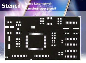
What Are PCB Stencils?
A PCB stencil is a thin sheet of material, typically stainless steel or polyester, with a pattern of openings that correspond to the pads on a PCB. The stencil is placed over the PCB, and solder paste is applied through the openings onto the pads. This process ensures that the correct amount of solder paste is deposited on each pad, making it easier to place components accurately and achieve reliable solder joints.
Types of PCB Stencils
There are two main types of PCB stencils:
- Stainless Steel Stencils: These are the most common type of stencils used in PCB Assembly. They are durable, reusable, and offer excellent precision. Stainless steel stencils are typically laser-cut or chemically etched.
- Polyester Stencils: These stencils are made from a thin, flexible material and are often used for low-volume or prototype PCB assembly. They are less durable than stainless steel stencils but are cheaper and easier to produce.
Why Use PCB Stencils?
Using a PCB stencil offers several benefits over applying solder paste manually:
- Consistency: Stencils ensure that the same amount of solder paste is applied to each pad, resulting in more consistent solder joints and better overall PCB Quality.
- Efficiency: Applying solder paste with a stencil is much faster than doing it manually, making it ideal for high-volume production.
- Precision: Stencils allow for precise solder paste application, even on small or closely spaced pads, which is essential for surface-mount devices (SMDs).
- Cost-effective: While there is an initial investment in creating a stencil, it can be reused multiple times, making it a cost-effective solution in the long run.

How to Make PCB Stencils
There are several methods for creating PCB stencils, each with its own advantages and disadvantages. Let’s explore the most common techniques:
Laser Cutting
Laser cutting is one of the most popular methods for creating stainless steel PCB stencils. This process involves using a high-powered laser to cut the stencil design into a sheet of stainless steel. Laser-Cut Stencils offer excellent precision and durability, making them suitable for high-volume production.
Advantages of Laser Cutting
- High precision
- Fast turnaround times
- Suitable for complex designs
- Durable and reusable
Disadvantages of Laser Cutting
- Higher cost compared to other methods
- Requires specialized equipment
- Not suitable for very fine pitch components
Chemical Etching
Chemical etching is another common method for creating stainless steel PCB stencils. In this process, a photoresist is applied to the stainless steel sheet, and the stencil design is transferred onto the photoresist using UV light. The exposed areas of the photoresist are then removed, and the stainless steel is etched using a chemical solution, leaving behind the stencil pattern.
Advantages of Chemical Etching
- Lower cost compared to laser cutting
- Suitable for fine pitch components
- Good precision
Disadvantages of Chemical Etching
- Slower turnaround times compared to laser cutting
- Requires careful handling of chemicals
- Not as durable as laser-cut stencils
3D Printing
3D printing is an emerging technology that can be used to create polyester PCB stencils. In this process, a 3D printer is used to print the stencil design using a special polyester material. 3D-printed stencils are ideal for low-volume production and prototyping.
Advantages of 3D Printing
- Low cost for small quantities
- Fast turnaround times
- Suitable for complex designs
Disadvantages of 3D Printing
- Lower durability compared to stainless steel stencils
- Not suitable for high-volume production
- Limited material options
Comparison of PCB Stencil Making Methods
| Method | Material | Precision | Durability | Cost | Turnaround Time |
|---|---|---|---|---|---|
| Laser Cutting | Stainless Steel | High | High | High | Fast |
| Chemical Etching | Stainless Steel | Good | Medium | Medium | Slow |
| 3D Printing | Polyester | Good | Low | Low | Fast |

Best Practices for Using PCB Stencils
To get the most out of your PCB stencils, follow these best practices:
- Choose the right stencil thickness: The stencil thickness should be based on the size of the components and the desired amount of solder paste. A common thickness for SMD stencils is 0.1 mm (4 mil).
- Align the stencil properly: Ensure that the stencil is aligned correctly with the PCB to avoid misplaced solder paste. Use alignment pins or fiducials to help with positioning.
- Use the correct solder paste: Choose a solder paste that is compatible with your components and has the right viscosity for your stencil.
- Apply solder paste evenly: Use a squeegee or automated solder paste dispenser to apply the paste evenly across the stencil. Maintain a consistent pressure and angle.
- Clean the stencil regularly: Clean your stencil after each use to prevent solder paste buildup and ensure consistent performance. Use a compatible cleaning solution and follow the manufacturer’s guidelines.

Frequently Asked Questions (FAQ)
- Q: Can I reuse a PCB stencil?
A: Yes, stainless steel PCB stencils can be reused multiple times with proper cleaning and storage. Polyester stencils are less durable and may need to be replaced more frequently. - Q: How do I choose the right stencil thickness?
A: The stencil thickness depends on the size of your components and the desired amount of solder paste. A common thickness for SMD stencils is 0.1 mm (4 mil), but thicker stencils may be needed for larger components. - Q: Can I make my own PCB stencil at home?
A: While it is possible to make a simple PCB stencil at home using materials like mylar or kapton film, the precision and durability will be limited. For best results, it is recommended to use professionally manufactured stainless steel or polyester stencils. - Q: How do I align the stencil with the PCB?
A: Use alignment pins or fiducials to help position the stencil correctly on the PCB. Some stencils come with pre-punched alignment holes that correspond to holes on the PCB. - Q: What is the best way to clean a PCB stencil?
A: Use a compatible cleaning solution, such as isopropyl alcohol or a specialized stencil cleaner, and follow the manufacturer’s guidelines. Avoid using abrasive materials that could damage the stencil. Regular cleaning helps prevent solder paste buildup and ensures consistent performance.
Conclusion
PCB stencils are a crucial tool for anyone serious about creating high-quality, professional PCBs. By understanding the different types of stencils, their advantages and disadvantages, and the various methods of creating them, you can choose the best option for your needs and budget.
Remember to follow best practices when using your PCB stencil, including choosing the right thickness, aligning it properly, using the correct solder paste, applying it evenly, and cleaning the stencil regularly. By doing so, you’ll be able to achieve consistent, reliable results and take your PCB assembly to the next level.
No responses yet