Introduction to PCB Buildup
Printed Circuit Boards (PCBs) are essential components in modern electronic devices. They provide a platform for interconnecting electronic components and enable the efficient transfer of signals and power. The buildup of a PCB refers to the layered structure of the board, which consists of conductive and insulating materials. Understanding the buildup of a PCB is crucial for designers, manufacturers, and engineers to ensure optimal performance, reliability, and manufacturability of electronic products.
Key Components of PCB Buildup
The buildup of a PCB typically consists of the following key components:
-
Substrate: The substrate is the base material of the PCB, usually made of a dielectric material such as FR-4, which is a glass-reinforced epoxy laminate. The substrate provides mechanical support and electrical insulation between the conductive layers.
-
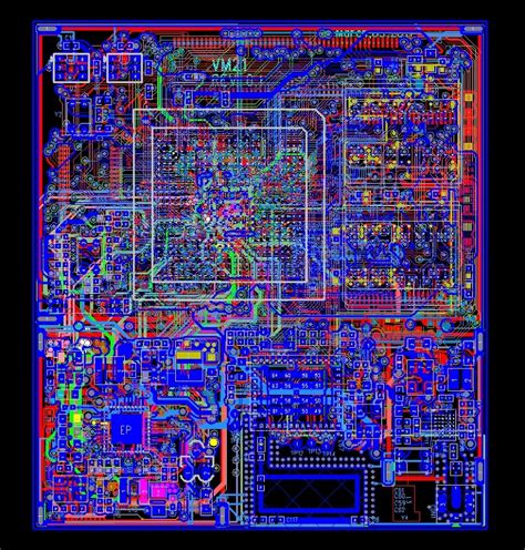
Copper Layers: Copper layers are the conductive paths that carry electrical signals and power throughout the PCB. The number of copper layers varies depending on the complexity and requirements of the circuit design. Each copper layer is etched to create the desired circuit pattern.
-
Solder Mask: The solder mask is a protective coating applied over the copper layers, leaving only the exposed areas where components will be soldered. It helps prevent short circuits and provides insulation between the copper traces. Solder mask is typically green in color but can also be found in other colors like red, blue, or black.
-
Silkscreen: The silkscreen is a printed layer on top of the solder mask that provides text, logos, and component identifiers. It helps in the assembly process and provides a visual reference for the placement of components on the PCB.
-
Vias: Vias are small holes drilled through the PCB to interconnect different copper layers. They allow signals to travel vertically between layers, enabling more complex routing and compact designs. Vias can be through-hole (going through all layers) or blind/buried (connecting only certain layers).

Types of PCB Buildup
There are several types of PCB buildup, each with its own characteristics and advantages. The choice of buildup depends on factors such as the complexity of the circuit, the required performance, and the manufacturing constraints. Some common types of PCB buildup include:
-
Single-Layer PCB: A single-layer PCB consists of a substrate with a single layer of copper on one side. It is the simplest and most cost-effective type of PCB, suitable for basic circuits with low complexity.
-
Double-Layer PCB: A double-layer PCB has copper layers on both sides of the substrate, allowing for more complex routing and higher component density compared to Single-Layer PCBs. The two layers are interconnected using through-hole vias.
-
Multi-Layer PCB: Multi-layer PCBs have three or more copper layers, with insulating layers sandwiched between them. They offer high density and complex routing capabilities, making them suitable for advanced electronic devices. The layers are interconnected using a combination of through-hole, blind, and buried vias.
-
High Density Interconnect (HDI) PCB: HDI PCBs feature fine pitch traces, small vias, and high layer counts. They enable the development of compact and high-performance electronic devices. HDI PCBs often incorporate microvias, which are small laser-drilled vias that interconnect adjacent layers.

PCB Buildup Manufacturing Process
The manufacturing process of a PCB involves several steps to create the desired buildup. The general steps in the PCB buildup manufacturing process are as follows:
-
Substrate Preparation: The substrate material is cut to the required size and shape. Copper foils are laminated onto the substrate using heat and pressure.
-
Drilling: Holes are drilled through the substrate and copper layers to create vias and component mounting holes. The drilling process can be done mechanically or using laser technology for smaller and more precise holes.
-
Plating: The drilled holes are plated with a conductive material, typically copper, to establish electrical connections between layers. This process is known as through-hole plating.
-
Patterning: The desired circuit pattern is transferred onto the copper layers using a photoresist and exposure to light. The unexposed areas are etched away, leaving the desired copper traces.
-
Solder Mask Application: The solder mask is applied over the copper layers, leaving only the areas where components will be soldered exposed. The solder mask is typically applied using a screen-printing process.
-
Silkscreen Printing: The silkscreen layer is printed on top of the solder mask, providing text, logos, and component identifiers. This process is also done using screen printing.
-
Surface Finish: A surface finish is applied to the exposed copper areas to protect them from oxidation and enhance solderability. Common surface finishes include Hot Air Solder Leveling (HASL), Electroless Nickel Immersion Gold (ENIG), and Immersion Silver.
-
Electrical Testing: The manufactured PCB undergoes electrical testing to ensure the integrity of the connections and the absence of short circuits or open connections. This step is critical to guarantee the functionality and reliability of the PCB.

Factors Affecting PCB Buildup Design
When designing the buildup of a PCB, several factors need to be considered to ensure optimal performance and manufacturability. Some of these factors include:
-
Circuit Requirements: The complexity and performance requirements of the circuit dictate the number of layers, the routing density, and the type of vias needed in the PCB buildup.
-
Signal Integrity: Signal integrity is crucial in high-speed and high-frequency applications. The PCB buildup should be designed to minimize signal losses, crosstalk, and reflections. Factors such as trace width, spacing, and dielectric material properties play a significant role in maintaining signal integrity.
-
Thermal Management: Heat dissipation is a critical aspect of PCB design, especially for high-power applications. The PCB buildup should incorporate thermal management techniques such as the use of thermal vias, copper pours, and heat sinks to effectively dissipate heat and prevent component failure.
-
Manufacturing Constraints: The PCB buildup design must consider the limitations and capabilities of the manufacturing process. Factors such as minimum trace width, spacing, and hole size should adhere to the manufacturing tolerances to ensure reliable and cost-effective production.
-
Cost Considerations: The choice of PCB buildup directly impacts the overall cost of the PCB. Factors such as the number of layers, the type of vias, and the surface finish selected affect the manufacturing cost. It is essential to strike a balance between performance requirements and cost-effectiveness.
Advanced PCB Buildup Techniques
As electronic devices become more complex and demanding, advanced PCB buildup techniques have emerged to address the challenges of high-density interconnects and high-speed signaling. Some of these advanced techniques include:
-
Embedded Components: Embedded components, such as capacitors and resistors, are placed within the PCB substrate rather than on the surface. This technique saves space, reduces parasitic effects, and improves signal integrity.
-
Via-in-Pad: Via-in-pad is a technique where vias are placed directly under the component pads, allowing for higher component density and improved routing efficiency. This technique requires precise manufacturing processes to ensure reliable connections.
-
Blind and Buried Vias: Blind vias connect an outer layer to an inner layer, while buried vias connect two or more inner layers without reaching the outer layers. These types of vias enable more efficient use of space and improved signal integrity in multi-layer PCBs.
-
Microvias: Microvias are small laser-drilled vias that interconnect adjacent layers in HDI PCBs. They offer high-density interconnects and enable the development of compact and high-performance electronic devices.
-
Controlled Impedance: Controlled impedance is a technique used to maintain consistent impedance along the signal path, minimizing reflections and ensuring signal integrity. It involves precise control of the trace width, spacing, and dielectric material properties.
PCB Buildup Standards and Guidelines
To ensure consistency and reliability in PCB manufacturing, several standards and guidelines have been established. These standards provide recommendations for PCB design, materials, and manufacturing processes. Some of the widely recognized standards include:
-
IPC Standards: The Institute of Printed Circuits (IPC) is a global trade association that develops and maintains standards for the electronic interconnect industry. IPC standards cover various aspects of PCB design, fabrication, and assembly, such as IPC-2221 for design, IPC-6012 for qualification and performance, and IPC-A-600 for acceptability.
-
JEDEC Standards: The Joint Electron Device Engineering Council (JEDEC) is an independent semiconductor engineering trade organization and standardization body. JEDEC standards cover a wide range of electronic components, including PCBs. For example, JEDEC-95 provides guidelines for PCB design and manufacturing.
-
Mil-Spec Standards: Military specifications (Mil-Spec) are standards developed by the United States Department of Defense for PCBs used in military and aerospace applications. These standards have stringent requirements for quality, reliability, and performance. Examples include MIL-P-55110 for rigid PCBs and MIL-P-50884 for flexible PCBs.
Frequently Asked Questions (FAQ)
-
What is the difference between a single-layer and a double-layer PCB?
A single-layer PCB has a copper layer on only one side of the substrate, while a double-layer PCB has copper layers on both sides. Double-layer PCBs offer more routing options and higher component density compared to single-layer PCBs. -
What is the purpose of vias in a PCB?
Vias are small holes drilled through the PCB to interconnect different copper layers. They allow signals to travel vertically between layers, enabling more complex routing and compact designs. -
What is the role of the solder mask in a PCB?
The solder mask is a protective coating applied over the copper layers, leaving only the exposed areas where components will be soldered. It helps prevent short circuits and provides insulation between the copper traces. -
What factors should be considered when choosing the buildup of a PCB?
Factors to consider when choosing the PCB buildup include the complexity of the circuit, the required performance, signal integrity, thermal management, manufacturing constraints, and cost considerations. -
What are the benefits of using advanced PCB buildup techniques like embedded components and microvias?
Advanced PCB buildup techniques offer several benefits, such as saving space, reducing parasitic effects, improving signal integrity, and enabling the development of compact and high-performance electronic devices.
Conclusion
Understanding the buildup of a PCB is essential for designing, manufacturing, and utilizing electronic devices effectively. The layered structure of a PCB, consisting of conductive and insulating materials, plays a crucial role in the performance, reliability, and manufacturability of electronic products. By considering factors such as circuit requirements, signal integrity, thermal management, and manufacturing constraints, designers can create optimal PCB buildups that meet the specific needs of their applications.
As technology advances, new techniques and materials continue to emerge in PCB manufacturing, enabling the development of more complex and high-performance electronic devices. Staying updated with industry standards, guidelines, and best practices is crucial for engineers and manufacturers to ensure the production of reliable and efficient PCBs.
By mastering the concepts of PCB buildup, designers and engineers can unlock the full potential of electronic devices, driving innovation and shaping the future of technology.
| Type of PCB Buildup | Layers | Advantages | Disadvantages |
|---|---|---|---|
| Single-Layer PCB | 1 | Low cost, simple design | Limited routing options, low component density |
| Double-Layer PCB | 2 | Improved routing, higher component density | Higher cost compared to single-layer PCBs |
| Multi-Layer PCB | 3 or more | High density, complex routing capabilities | Increased cost, manufacturing complexity |
| HDI PCB | Multiple, with microvias | Compact size, high performance | Higher cost, advanced manufacturing processes required |
No responses yet