Introduction to PCB Stackups
A printed circuit board (PCB) stackup refers to the arrangement of copper and insulating layers that make up a PCB. The stackup defines the number of layers, the thickness of each layer, and the materials used. Choosing the right PCB stackup is crucial for ensuring proper functionality, signal integrity, and manufacturability of the board.
In this article, we will explore the standard stackups for Multilayer PCBs, focusing on the offerings from RAYPCB, a leading PCB manufacturer. We will discuss the advantages and considerations for different stackup configurations, as well as answer frequently asked questions about PCB stackups.
Why is the PCB Stackup Important?
The PCB stackup plays a critical role in the performance and reliability of a circuit board. Here are some reasons why the stackup is so important:
-
Signal Integrity: The arrangement of layers and the spacing between them affects the signal integrity of the PCB. Proper stackup design helps minimize crosstalk, signal reflections, and electromagnetic interference (EMI).
-
Impedance Control: The stackup determines the characteristic impedance of the traces on the PCB. Maintaining consistent impedance is essential for high-speed designs to prevent signal distortion and ensure proper termination.
-
Power Distribution: The stackup also influences the power distribution network (PDN) of the PCB. Adequate copper thickness and proper placement of power and ground planes are necessary for delivering clean and stable power to components.
-
Manufacturability: The choice of materials, layer thicknesses, and the overall stackup affects the manufacturability of the PCB. A well-designed stackup ensures that the board can be fabricated reliably and cost-effectively.

Standard Stackups for Multilayer PCBs
RAYPCB offers several standard stackups for multilayer PCBs, catering to different design requirements and budgets. Let’s explore some of the most common stackups:
4-Layer PCB Stackup
The 4-layer PCB stackup is a popular choice for many designs due to its balance of cost and performance. Here’s a typical 4-layer stackup:
| Layer | Material | Thickness |
|---|---|---|
| Top Layer | Copper | 1 oz (35 μm) |
| Dielectric Layer 1 | FR-4 | 0.2 mm |
| Inner Layer 1 | Copper | 1 oz (35 μm) |
| Core | FR-4 | 1.6 mm |
| Inner Layer 2 | Copper | 1 oz (35 μm) |
| Dielectric Layer 2 | FR-4 | 0.2 mm |
| Bottom Layer | Copper | 1 oz (35 μm) |
In this stackup, the top and bottom layers are used for component placement and routing, while the inner layers are typically used for power and ground planes. The FR-4 core provides mechanical stability and insulation between the layers.
Advantages of the 4-layer stackup:
– Cost-effective compared to higher layer count boards
– Suitable for most low to medium complexity designs
– Allows for adequate signal routing and power distribution
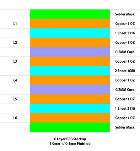
6-Layer PCB Stackup
For designs that require more routing space or better signal integrity, a 6-layer PCB stackup is often used. Here’s an example of a 6-layer stackup:
| Layer | Material | Thickness |
|---|---|---|
| Top Layer | Copper | 1 oz (35 μm) |
| Dielectric Layer 1 | FR-4 | 0.2 mm |
| Inner Layer 1 | Copper | 1 oz (35 μm) |
| Core 1 | FR-4 | 0.8 mm |
| Inner Layer 2 | Copper | 1 oz (35 μm) |
| Dielectric Layer 2 | FR-4 | 0.2 mm |
| Inner Layer 3 | Copper | 1 oz (35 μm) |
| Core 2 | FR-4 | 0.8 mm |
| Inner Layer 4 | Copper | 1 oz (35 μm) |
| Dielectric Layer 3 | FR-4 | 0.2 mm |
| Bottom Layer | Copper | 1 oz (35 μm) |
In this stackup, the additional inner layers provide more routing space and allow for dedicated power and ground planes. The two FR-4 cores offer increased mechanical strength and help maintain a symmetrical stackup.
Advantages of the 6-layer stackup:
– Increased routing density compared to 4-layer boards
– Dedicated power and ground planes for better power integrity
– Improved signal integrity due to the ability to route critical signals on inner layers
8-Layer and Higher PCB Stackups
For complex designs with high component density, high-speed signals, or advanced packaging requirements, 8-layer or higher PCB stackups are often necessary. These stackups follow a similar pattern to the 6-layer stackup, with additional inner layers and dielectric layers.
Here’s an example of an 8-layer stackup:
| Layer | Material | Thickness |
|---|---|---|
| Top Layer | Copper | 1 oz (35 μm) |
| Dielectric Layer 1 | FR-4 | 0.2 mm |
| Inner Layer 1 | Copper | 1 oz (35 μm) |
| Core 1 | FR-4 | 0.6 mm |
| Inner Layer 2 | Copper | 1 oz (35 μm) |
| Dielectric Layer 2 | FR-4 | 0.2 mm |
| Inner Layer 3 | Copper | 1 oz (35 μm) |
| Core 2 | FR-4 | 0.6 mm |
| Inner Layer 4 | Copper | 1 oz (35 μm) |
| Dielectric Layer 3 | FR-4 | 0.2 mm |
| Inner Layer 5 | Copper | 1 oz (35 μm) |
| Core 3 | FR-4 | 0.6 mm |
| Inner Layer 6 | Copper | 1 oz (35 μm) |
| Dielectric Layer 4 | FR-4 | 0.2 mm |
| Bottom Layer | Copper | 1 oz (35 μm) |
Advantages of 8-layer and higher stackups:
– Increased routing density for complex designs
– Multiple dedicated power and ground planes for improved power integrity
– Ability to route high-speed signals on inner layers with proper reference planes
– Accommodation for advanced packaging techniques, such as Ball Grid Arrays (BGAs) and chip-scale packages (CSPs)

Considerations for Choosing a PCB Stackup
When selecting a PCB stackup for your design, there are several factors to consider:
-
Design Complexity: The complexity of your design, including the number of components, routing density, and signal requirements, will influence the choice of stackup. More complex designs typically require higher layer counts.
-
Signal Integrity: Consider the signal integrity requirements of your design. High-speed designs may benefit from dedicated signal layers, proper reference planes, and controlled impedance traces.
-
Power Distribution: Evaluate the power distribution needs of your design. Higher layer count stackups allow for dedicated power and ground planes, which can improve power integrity and reduce noise.
-
Cost: The cost of the PCB increases with the number of layers. Consider the budget constraints of your project and choose a stackup that balances cost and performance.
-
Manufacturability: Discuss your stackup requirements with your PCB manufacturer to ensure that it can be fabricated reliably and cost-effectively. Some stackups may require special materials or processes that can impact cost and lead time.

FAQ
1. What is the most common PCB stackup?
The most common PCB stackup is the 4-layer stackup, which consists of a top layer, two inner layers, and a bottom layer. This stackup offers a good balance of cost and performance for many designs.
2. How does the PCB stackup affect signal integrity?
The PCB stackup affects signal integrity in several ways. The spacing between layers, the arrangement of signal and reference planes, and the dielectric materials used all influence signal propagation, crosstalk, and EMI. Proper stackup design helps minimize these issues and ensures reliable signal transmission.
3. Can I mix different dielectric materials in a PCB stackup?
Yes, it is possible to mix different dielectric materials in a PCB stackup. This is often done to achieve specific electrical properties or to optimize the stackup for certain frequencies. However, mixing materials can increase the complexity and cost of the PCB fabrication process.
4. How do I choose the right copper thickness for my PCB stackup?
The choice of copper thickness depends on several factors, including the current carrying requirements, trace width, and thermal management needs of your design. Thicker copper layers can carry more current and help dissipate heat, but they also increase the cost and weight of the PCB. A common copper thickness is 1 oz (35 μm), but thicker options, such as 2 oz (70 μm) or even 4 oz (140 μm), are available for high-current applications.
5. What are the benefits of using a symmetrical PCB stackup?
A symmetrical PCB stackup, where the layer arrangement is mirrored around the center of the board, offers several benefits. It helps minimize warpage and mechanical stress during fabrication and assembly, as the forces are balanced on both sides of the board. Additionally, a symmetrical stackup can improve signal integrity by providing consistent reference planes for signal layers.
Conclusion
Choosing the right PCB stackup is essential for ensuring the functionality, reliability, and manufacturability of your design. RAYPCB offers a range of standard stackups for multilayer PCBs, including 4-layer, 6-layer, 8-layer, and higher options. When selecting a stackup, consider factors such as design complexity, signal integrity, power distribution, cost, and manufacturability.
By understanding the importance of the PCB stackup and working closely with your PCB manufacturer, you can make informed decisions that will help optimize your design and achieve the best possible results.
No responses yet