Introduction to PCB Stackup
A printed circuit board (PCB) stackup refers to the arrangement of copper and insulating layers that make up a PCB. The stackup defines the number of layers, their order, and the materials used for each layer. Designing an appropriate PCB stackup is crucial for ensuring proper functionality, signal integrity, and manufacturability of the circuit board.
Key Considerations in PCB Stackup Design
When designing a PCB stackup, several key factors must be considered:
- Number of layers
- Layer order and arrangement
- Material selection
- Thickness of each layer
- Copper weight
- Dielectric constant and loss tangent
- Impedance control
- Via and pad sizes
- Manufacturing constraints
- Cost
Types of PCB Stackups
There are several common types of PCB stackups, each with its own advantages and applications.
Single-Layer PCB Stackup
A single-layer PCB consists of a single conductive layer, usually made of copper, laminated onto an insulating substrate. Single-Layer PCBs are the simplest and most cost-effective option, suitable for basic circuits with low complexity.
| Layer | Material | Thickness (mm) |
|---|---|---|
| Top | Copper | 0.035 |
| Core | FR-4 | 1.6 |
Double-Layer PCB Stackup
Double-layer PCBs have two conductive layers, one on each side of the insulating substrate. This allows for more complex circuits and better signal routing compared to single-layer boards.
| Layer | Material | Thickness (mm) |
|---|---|---|
| Top | Copper | 0.035 |
| Core | FR-4 | 1.6 |
| Bottom | Copper | 0.035 |
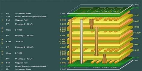
Multi-Layer PCB Stackup
Multi-layer PCBs consist of three or more conductive layers, alternating with insulating layers. This allows for even more complex circuits, higher component density, and better signal integrity. Common multi-layer stackups include 4-layer, 6-layer, 8-layer, and 10-layer boards.
Example of a 4-layer PCB stackup:
| Layer | Material | Thickness (mm) |
|---|---|---|
| Top | Copper | 0.035 |
| Prepreg | FR-4 | 0.2 |
| Inner1 | Copper | 0.035 |
| Core | FR-4 | 1.2 |
| Inner2 | Copper | 0.035 |
| Prepreg | FR-4 | 0.2 |
| Bottom | Copper | 0.035 |

Material Selection for PCB Stackup
Choosing the right materials for your PCB stackup is essential for achieving the desired performance and reliability.
Conductive Materials
The most common conductive material used in PCBs is copper. Copper thickness is typically measured in ounces per square foot (oz/ft²), with common weights being 0.5 oz, 1 oz, and 2 oz.
Insulating Materials
The insulating layers in a PCB stackup are typically made of FR-4, a flame-retardant glass-reinforced epoxy laminate. Other materials, such as Rogers or Isola, may be used for high-frequency or high-speed applications.
Dielectric Properties
The dielectric constant (Dk) and loss tangent (Df) of the insulating material affect the signal propagation and loss in the PCB. Lower Dk and Df values are generally preferred for high-speed designs.
| Material | Dk | Df |
|---|---|---|
| FR-4 | 4.5 | 0.02 |
| Rogers | 2.2 | 0.0009 |
| Isola | 3.0 | 0.0035 |

Signal Integrity in PCB Stackup Design
Ensuring signal integrity is crucial for the proper functioning of high-speed and high-frequency circuits. PCB stackup design plays a significant role in maintaining signal integrity.
Impedance Control
Controlling the characteristic impedance of transmission lines is essential for minimizing reflections and signal distortion. This is achieved by adjusting the trace width, thickness, and spacing, as well as the dielectric properties of the insulating layers.
Crosstalk Reduction
Crosstalk occurs when signals from one trace interfere with adjacent traces. To minimize crosstalk, designers can:
- Increase spacing between traces
- Use guard traces or ground planes
- Route sensitive signals on different layers
- Use differential signaling
Via Design
Vias are used to connect traces on different layers of the PCB. Proper via design is crucial for minimizing signal distortion and reflections. Designers should consider:
- Via size and drill diameter
- Via placement and spacing
- Via stubs and their impact on signal integrity
- Back-drilling or blind/buried vias for high-speed signals

Power Distribution in PCB Stackup
An effective power distribution network (PDN) is essential for providing clean, stable power to all components on the PCB.
Power and Ground Planes
Dedicated power and ground planes help distribute power evenly across the board and provide a low-impedance return path for signals. These planes also act as shields, reducing electromagnetic interference (EMI) and crosstalk.
Decoupling Capacitors
Decoupling capacitors are used to provide local, high-frequency power supply filtering for components. Proper placement and selection of decoupling capacitors are crucial for maintaining power integrity.
Splitting Power and Ground Planes
In some cases, it may be necessary to split power and ground planes to isolate different sections of the circuit. This can help prevent noise coupling and improve power integrity.
Thermal Management in PCB Stackup
Thermal management is an important consideration in PCB stackup design, particularly for high-power circuits.
Copper Thickness and Heat Dissipation
Thicker copper layers can help dissipate heat more effectively. Designers can use thicker copper on power and ground planes, or even dedicated thermal layers, to improve thermal performance.
Thermal Vias
Thermal vias are used to transfer heat from components to the opposite side of the board or to internal copper planes. They help spread heat more evenly across the PCB and improve overall thermal performance.
Manufacturing Considerations in PCB Stackup Design
Designing a PCB stackup that is easy to manufacture can help reduce costs and improve reliability.
Layer Count and Board Thickness
Increasing the number of layers and overall board thickness can make the PCB more challenging and expensive to manufacture. Designers should strive to minimize layer count and thickness while still meeting performance requirements.
Material Availability and Cost
Some specialized materials, such as high-frequency laminates, may be more expensive or have longer lead times. Designers should consider material availability and cost when selecting materials for the stackup.
Design for Manufacturing (DFM)
Adhering to DFM guidelines, such as minimum trace width and spacing, via size, and pad dimensions, can help ensure that the PCB can be manufactured reliably and cost-effectively.
Frequently Asked Questions
- What is the difference between a single-layer and a double-layer PCB stackup?
-
A single-layer PCB has only one conductive layer, while a double-layer PCB has two conductive layers, one on each side of the insulating substrate. Double-layer PCBs allow for more complex circuits and better signal routing compared to single-layer boards.
-
What factors should be considered when selecting materials for a PCB stackup?
-
When selecting materials for a PCB stackup, designers should consider the dielectric properties (Dk and Df), thermal performance, mechanical strength, and cost of the materials. The choice of materials will depend on the specific requirements of the application, such as high-speed performance, thermal management, or cost constraints.
-
How can signal integrity be maintained in a PCB stackup design?
-
Signal integrity can be maintained in a PCB stackup design by controlling the characteristic impedance of transmission lines, minimizing crosstalk through proper trace spacing and routing, and optimizing via design to minimize signal distortion and reflections. Additionally, using dedicated power and ground planes can help provide a stable reference for signals and reduce electromagnetic interference.
-
Why is thermal management important in PCB stackup design?
-
Thermal management is important in PCB stackup design because it helps ensure that the circuit operates within its specified temperature range and prevents overheating, which can lead to component failure or reduced reliability. Effective thermal management can be achieved through the use of thicker copper layers, dedicated thermal layers, and thermal vias to dissipate heat away from components.
-
What are some manufacturing considerations for PCB stackup design?
- When designing a PCB stackup, it is important to consider manufacturing constraints such as minimum trace width and spacing, via size and drill diameter, and pad dimensions. Adhering to design for manufacturing (DFM) guidelines can help ensure that the PCB can be manufactured reliably and cost-effectively. Additionally, minimizing layer count and board thickness where possible can help reduce manufacturing costs and complexity.
Conclusion
Designing an effective PCB stackup is essential for ensuring the proper functioning, signal integrity, and manufacturability of a circuit board. By considering factors such as the number of layers, material selection, signal integrity, power distribution, thermal management, and manufacturing constraints, designers can create PCB stackups that meet the specific requirements of their applications. A well-designed PCB stackup can help minimize signal distortion, reduce electromagnetic interference, and improve overall system performance and reliability.
No responses yet