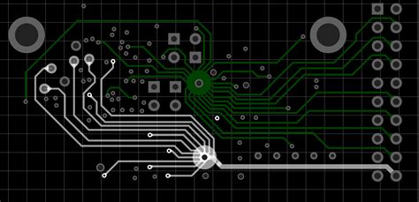
Understanding the Basics of PCB Routing
Before diving into specific routing techniques, it’s essential to understand the basics of PCB routing. PCB routing is the process of creating the copper traces that connect the components on a PCB. These traces carry electrical signals between components, and their design can significantly impact the performance and reliability of the final product.
Types of PCB Routing
There are two main types of PCB routing:
- Manual Routing: In manual routing, the designer manually creates each trace on the PCB using specialized software. This approach allows for greater control over the routing process but can be time-consuming and requires a high level of skill.
- Autorouting: Autorouting involves using software algorithms to automatically create the traces on the PCB. While autorouting can save time, it may not always produce the most optimal results and may require manual adjustments.
PCB Layers
PCBs can have multiple layers, each containing copper traces. The number of layers in a PCB depends on the complexity of the design and the available space. Common PCB layer configurations include:
| Layers | Description |
|---|---|
| 1 | Single-Sided PCB, components on one side, traces on the other |
| 2 | Double-sided PCB, components and traces on both sides |
| 4 | Four-layer PCB, two inner layers for power and ground planes |
| 6+ | Multi-layer PCBs for complex designs, additional signal layers |
Planning Your PCB Layout
Before beginning the routing process, it’s crucial to plan your PCB layout carefully. A well-planned layout can simplify routing and improve the overall performance of the board.
Component Placement
Start by placing the components on the PCB in a logical manner. Consider the following factors when placing components:
- Functionality: Group related components together to minimize the length of traces and improve signal integrity.
- Size: Place larger components first, as they can be more challenging to position later in the design process.
- Orientation: Ensure that components are oriented correctly, taking into account any required connections or clearances.
Power and Ground Planes
In multi-layer PCBs, dedicate one or more layers to power and ground planes. These planes provide a low-impedance path for power distribution and help to reduce EMI. When planning your layout, consider the following:
- Plane Thickness: Thicker planes offer lower impedance and better current-carrying capacity.
- Via Placement: Place vias strategically to connect the power and ground planes to the components on the signal layers.

Routing Techniques
Once you have planned your PCB layout, it’s time to start routing the traces. Here are some essential techniques to keep in mind:
Trace Width and Spacing
The width and spacing of traces can affect signal integrity and EMI. When routing traces, consider the following:
- Current-Carrying Capacity: Wider traces can carry more current and generate less heat.
- Impedance Control: Maintain consistent trace widths and spacing to control impedance and minimize signal reflections.
- Clearance: Ensure adequate spacing between traces to prevent short circuits and minimize crosstalk.
Routing Angles
When routing traces, it’s generally best to use 45-degree angles rather than 90-degree angles. 45-degree angles minimize reflections and improve signal integrity. If 90-degree angles are unavoidable, use a chamfered corner to reduce the abruptness of the angle.
Via Placement
Vias are used to connect traces on different layers of the PCB. When placing vias, consider the following:
- Via Size: Smaller vias can save space but may be more difficult to manufacture reliably.
- Via Spacing: Ensure adequate spacing between vias to prevent short circuits and minimize crosstalk.
- Via Stubs: Minimize the length of via stubs to reduce signal reflections and improve signal integrity.
Length Matching
In high-speed designs, it’s essential to match the lengths of traces carrying related signals. Length matching ensures that signals arrive at their destinations at the same time, minimizing timing issues and signal integrity problems. When length matching, consider the following:
- Serpentine Routing: Use serpentine routing to add length to shorter traces, matching them to the longest trace in the group.
- Daisy-Chaining: Daisy-chain components to maintain consistent trace lengths between devices.

Dealing with EMI
Electromagnetic interference (EMI) can cause problems in PCB designs, leading to signal integrity issues and potentially violating regulatory requirements. Here are some techniques for minimizing EMI in your PCB design:
Shielding
Use shielding techniques to contain EMI generated by the PCB. Some common shielding methods include:
- Metal Enclosures: Place the PCB inside a metal enclosure to contain EMI.
- Shielding Cans: Use metal cans to shield specific components or areas of the PCB.
- Shielding Gaskets: Use conductive gaskets to ensure a proper electrical connection between the PCB and the enclosure.
Filtering
Implement filtering techniques to suppress EMI at its source. Some common filtering methods include:
- Decoupling Capacitors: Place decoupling capacitors near noise-generating components to suppress high-frequency noise.
- Ferrite Beads: Use ferrite beads to filter out high-frequency noise on power supply lines.
- Common Mode Chokes: Use common mode chokes to suppress common mode noise on signal lines.

Verifying Your Design
Once you have completed your PCB routing, it’s essential to verify your design before sending it for manufacturing. Here are some steps to take:
Design Rule Checking (DRC)
Use your PCB design software’s DRC tools to check for any design rule violations. DRC checks for issues such as:
- Trace Width and Spacing: Ensures that traces meet the specified width and spacing requirements.
- Via Size and Spacing: Checks that vias are the correct size and are spaced appropriately.
- Clearance: Verifies that there is adequate clearance between components and traces.
Signal Integrity Analysis
Perform signal integrity analysis to ensure that your design meets the required performance specifications. Signal integrity analysis tools can help you identify issues such as:
- Impedance Mismatch: Identifies areas where impedance mismatches may cause signal reflections.
- Crosstalk: Detects instances of crosstalk between adjacent traces.
- Timing Issues: Verifies that signals arrive at their destinations within the required time window.
FAQ
- Q: What is the difference between manual routing and autorouting?
A: Manual routing involves manually creating each trace on the PCB using specialized software, while autorouting uses software algorithms to automatically create the traces. Manual routing offers greater control but is time-consuming, while autorouting can save time but may not always produce optimal results. - Q: How do I choose the appropriate trace width for my PCB design?
A: The appropriate trace width depends on factors such as the current-carrying capacity, impedance control, and clearance requirements. Wider traces can carry more current and generate less heat, but they also take up more space. It’s essential to consult the manufacturer’s guidelines and use PCB design software to calculate the appropriate trace widths for your design. - Q: What is the purpose of power and ground planes in a PCB?
A: Power and ground planes provide a low-impedance path for power distribution and help to reduce electromagnetic interference (EMI). They are typically located on dedicated layers in multi-layer PCBs and are connected to the components on the signal layers using vias. - Q: Why is length matching important in high-speed PCB designs?
A: Length matching ensures that signals carried by related traces arrive at their destinations at the same time. This minimizes timing issues and signal integrity problems that can occur when signals arrive at different times. Length matching is particularly important in high-speed designs where timing is critical. - Q: How can I verify my PCB design before sending it for manufacturing?
A: You can verify your PCB design using design rule checking (DRC) and signal integrity analysis tools. DRC checks for design rule violations such as trace width and spacing, via size and spacing, and clearance issues. Signal integrity analysis tools can help identify issues such as impedance mismatch, crosstalk, and timing problems.
Conclusion
PCB routing is a critical step in the design of printed circuit boards, and it can be challenging for beginners. By understanding the basics of PCB routing, planning your layout carefully, and using the appropriate routing techniques, you can create reliable and high-performance PCBs. Remember to consider factors such as trace width and spacing, routing angles, via placement, and length matching when routing your PCB. Additionally, take steps to minimize EMI and verify your design before sending it for manufacturing. With practice and experience, PCB routing will become a more intuitive and efficient process.
No responses yet