Understanding Panelization and its Benefits
Panelization is a process in the manufacturing of printed circuit boards (PCBs) where multiple identical or different PCB designs are combined onto a single panel for production. This approach offers several benefits, including reduced manufacturing costs, improved efficiency, and better utilization of materials. By grouping multiple PCBs together, manufacturers can optimize the use of equipment, minimize handling, and streamline the assembly process.
Key Advantages of Panelization
- Cost reduction: Producing multiple PCBs on a single panel reduces the overall manufacturing cost per board.
- Increased efficiency: Panelization allows for faster production times and minimizes the need for manual handling of individual boards.
- Better material utilization: By arranging PCBs strategically on a panel, manufacturers can maximize the use of the substrate material, reducing waste.
- Simplified assembly: Panelized PCBs can be easily integrated into automated assembly lines, improving the speed and accuracy of the process.
Breakaway Tabs and Mouse Bites
To facilitate the separation of individual PCBs from the panelized array, manufacturers employ techniques such as breakaway tabs and mouse bites. These features allow for easy and clean separation of the boards without damaging the circuits or components.
Breakaway Tabs
Breakaway tabs, also known as break-off tabs or snap-off tabs, are small, removable sections that connect individual PCBs within a panel. These tabs are designed to be easily broken off after the manufacturing process is complete, allowing the boards to be separated from the panel. Breakaway tabs are typically located along the edges of the PCBs and are removed by applying gentle pressure or using a specialized tool.
Mouse Bites
Mouse bites, also referred to as perforations or v-cuts, are small, semi-circular cutouts along the edges of the PCBs within a panel. These cutouts create a series of weak points that allow for easy separation of the individual boards. Mouse bites are created using a specialized cutting tool during the panelization process and provide a clean and precise break when the boards are depanelized.

Designing for Panelization
When designing PCBs for panelization, several factors must be considered to ensure optimal results. These include the dimensions of the individual boards, the spacing between boards, and the placement of breakaway tabs or mouse bites.
Board Dimensions
The dimensions of the individual PCBs within a panel should be carefully planned to maximize the use of the available panel space. Standard panel sizes vary depending on the manufacturer and the specific requirements of the project. Common panel sizes include:
| Panel Size | Dimensions (mm) | Dimensions (inches) |
|---|---|---|
| Small | 100 x 100 | 3.94 x 3.94 |
| Medium | 200 x 200 | 7.87 x 7.87 |
| Large | 300 x 300 | 11.81 x 11.81 |
| Extra Large | 450 x 450 | 17.72 x 17.72 |
When determining the dimensions of the individual boards, consider the following:
- The size and shape of the PCB design
- The number of boards to be included in the panel
- The spacing required between boards for breakaway tabs or mouse bites
- Any additional features, such as tooling holes or fiducial marks
Spacing and Placement
Proper spacing between individual PCBs within a panel is crucial for ensuring clean and easy separation. The spacing requirements may vary depending on the chosen separation method (breakaway tabs or mouse bites) and the manufacturer’s guidelines.
Breakaway Tabs
When using breakaway tabs, consider the following:
- Tab width: The width of the breakaway tabs should be sufficient to hold the boards securely during manufacturing but narrow enough to allow for easy separation. Common tab widths range from 0.5 mm to 1.5 mm.
- Tab placement: Breakaway tabs should be placed strategically along the edges of the PCBs to provide adequate support and minimize the risk of damage during separation. Typically, tabs are placed at the corners and midpoints of the board edges.
- Tab spacing: The spacing between breakaway tabs should be consistent and sufficient to maintain the structural integrity of the panel. A common spacing range is 10 mm to 20 mm, depending on the size and weight of the boards.
Mouse Bites
When using mouse bites, consider the following:
- Bite size: The size of the mouse bites should be small enough to create weak points for easy separation but not so small that they compromise the stability of the panel during manufacturing. Common bite diameters range from 0.5 mm to 1.5 mm.
- Bite spacing: The spacing between mouse bites should be consistent and close enough to allow for easy separation. A common spacing range is 1 mm to 3 mm, depending on the thickness and material of the PCB.
- Bite placement: Mouse bites should be placed along the edges of the PCBs, typically at regular intervals. The placement should provide a balance between easy separation and maintaining the structural integrity of the panel.

Panelization Layout and Optimization
When creating the panelization layout, designers should aim to optimize the use of the available panel space while ensuring that the individual PCBs can be easily separated and meet the required specifications.
Panel Utilization
To maximize panel utilization, consider the following strategies:
- Arrange PCBs in a grid pattern: Place the individual boards in rows and columns to create a uniform and efficient layout.
- Minimize waste: Optimize the spacing between boards and the placement of breakaway tabs or mouse bites to reduce the amount of unused panel space.
- Consider mixed panelization: If the project involves different PCB designs, consider combining them on a single panel to optimize material usage and reduce production costs.
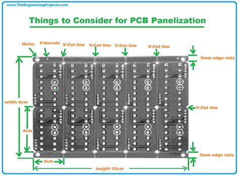
Tooling and Fiducial Marks
In addition to the PCB Layout, panelization designs should include tooling and fiducial marks to assist with the manufacturing and assembly processes.
- Tooling holes: These are small holes placed in the corners or edges of the panel that help to align and secure the panel during manufacturing. Common sizes for tooling holes range from 2 mm to 5 mm in diameter.
- Fiducial marks: These are precise reference points on the panel that help to align the PCBs during the assembly process. Fiducial marks are typically small, circular, or cross-shaped features placed near the corners or edges of the individual boards.
Panelization Software and Tools
To streamline the panelization design process, designers can use specialized software and tools that offer features specific to panel creation and optimization. Some popular panelization software options include:
- Altium Designer: A comprehensive PCB design software that includes panelization tools and features.
- Zuken CR-8000: A PCB design platform that offers advanced panelization capabilities and automation.
- Ucamco PanelShop: A dedicated panelization software that provides a range of tools for panel creation, optimization, and data preparation.
These tools help designers to create efficient panel layouts, optimize material usage, and ensure that the panelized PCBs meet the required specifications.

Best Practices for Panelization
To ensure successful panelization and high-quality PCBs, consider the following best practices:
- Collaborate with the manufacturer: Work closely with the PCB manufacturer to understand their specific requirements, guidelines, and recommendations for panelization.
- Consider the assembly process: When designing the panel layout, take into account the requirements of the assembly process, such as the placement of components and the orientation of the boards.
- Test the panelization design: Before finalizing the panel layout, create prototypes or test panels to validate the design and ensure that the PCBs can be easily separated without damage.
- Optimize for manufacturing efficiency: Aim to create panel layouts that maximize the number of PCBs per panel while minimizing waste and ensuring that the boards meet the required specifications.
- Document the panelization process: Maintain clear and detailed documentation of the panelization design, including the dimensions, spacing, and placement of breakaway tabs or mouse bites.
By following these best practices and carefully considering the dimensions and layout of the panelized PCBs, designers can create efficient and cost-effective solutions for PCB manufacturing.
Frequently Asked Questions (FAQ)
-
What is the minimum spacing required between PCBs in a panel?
The minimum spacing between PCBs in a panel depends on the chosen separation method and the manufacturer’s guidelines. For breakaway tabs, a common spacing range is 10 mm to 20 mm, while for mouse bites, the spacing typically ranges from 1 mm to 3 mm. -
Can different PCB designs be combined on the same panel?
Yes, different PCB designs can be combined on the same panel through a process called mixed panelization. This approach helps to optimize material usage and reduce production costs by manufacturing multiple designs simultaneously. -
What are the benefits of using panelization software?
Panelization software offers several benefits, including the ability to create efficient panel layouts, optimize material usage, and ensure that the panelized PCBs meet the required specifications. These tools often include features specifically designed for panel creation and optimization, streamlining the design process. -
How do I choose between breakaway tabs and mouse bites for my panelization design?
The choice between breakaway tabs and mouse bites depends on factors such as the size and thickness of the PCBs, the required separation force, and the manufacturer’s capabilities. Consult with your PCB manufacturer to determine the most suitable option for your specific project. -
Can panelization be used for both prototyping and high-volume production?
Yes, panelization can be used for both prototyping and high-volume production. In prototyping, panelization can help to reduce costs and lead times by allowing multiple designs to be manufactured simultaneously. In high-volume production, panelization is essential for optimizing manufacturing efficiency and reducing overall costs.
By understanding the dimensions, spacing, and best practices for panelization with breakaway tabs and mouse bites, designers can create efficient and cost-effective PCB designs that meet the requirements of their specific projects.
No responses yet