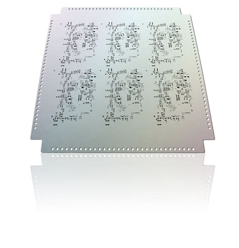
Introduction to PCB stencil Openings
When it comes to manufacturing printed circuit boards (PCBs), creating accurate and precise openings on the stencil is crucial for ensuring the quality and functionality of the final product. PCB Stencils are thin metal sheets with cutouts that allow solder paste to be applied to specific areas on the PCB during the assembly process. The openings on the stencil must be carefully designed and created to ensure that the correct amount of solder paste is deposited on the pads, leading to a reliable and efficient soldering process.
In this article, we will explore the five best tips for creating openings on PCB stencils, helping you achieve optimal results in your PCB manufacturing process.
Tip 1: Choose the Right Stencil Thickness
Understanding Stencil Thickness
The thickness of the PCB stencil plays a significant role in determining the amount of solder paste deposited on the pads. Choosing the right stencil thickness is essential for achieving the desired solder paste volume and ensuring a successful soldering process.
Factors Affecting Stencil Thickness Selection
When selecting the appropriate stencil thickness, consider the following factors:
- Component pitch and size
- Solder paste type and viscosity
- PCB Surface Finish
- Manufacturing process requirements
Recommended Stencil Thicknesses
The table below provides general guidelines for selecting PCB stencil thicknesses based on component pitch:
| Component Pitch | Recommended Stencil Thickness |
|---|---|
| > 0.65 mm | 0.100 mm – 0.150 mm |
| 0.50 mm – 0.65 mm | 0.100 mm – 0.125 mm |
| 0.40 mm – 0.50 mm | 0.075 mm – 0.100 mm |
| < 0.40 mm | 0.050 mm – 0.075 mm |

Tip 2: Optimize Aperture Design
Aperture Shape and Size
The shape and size of the apertures on the PCB stencil directly influence the solder paste deposit and the resulting solder joint. Optimizing the aperture design ensures that the correct amount of solder paste is applied to the pads, leading to reliable and consistent solder joints.
Common Aperture Shapes
- Square: Suitable for most SMD components
- Rectangular: Used for fine-pitch components and connectors
- Circular: Employed for ball grid array (BGA) components
- Oblong: Utilized for larger SMD components and connectors
Aperture Size Calculation
To calculate the appropriate aperture size, use the following formula:
Aperture Size = Pad Size + 2 × Solder Mask Expansion
Ensure that the aperture size allows for sufficient solder paste release while preventing bridging between adjacent pads.

Tip 3: Implement Proper Aperture Spacing
Importance of Aperture Spacing
Proper aperture spacing on the PCB stencil is crucial for preventing solder paste bridging and ensuring accurate solder paste deposition. Insufficient spacing between apertures can lead to solder paste bleeding and short circuits, while excessive spacing may result in insufficient solder paste volume on the pads.
Minimum Aperture Spacing Guidelines
The table below provides minimum aperture spacing guidelines based on stencil thickness:
| Stencil Thickness | Minimum Aperture Spacing |
|---|---|
| 0.100 mm – 0.150 mm | 0.150 mm |
| 0.075 mm – 0.100 mm | 0.125 mm |
| 0.050 mm – 0.075 mm | 0.100 mm |
Adjusting Aperture Spacing
When designing the PCB stencil, consider the following factors to optimize aperture spacing:
- Component density and placement
- Solder paste type and viscosity
- Manufacturing process capabilities
- PCB surface finish
Collaborate with your PCB manufacturer to determine the ideal aperture spacing for your specific project.

Tip 4: Incorporate Stencil Fiducials
Importance of Stencil Fiducials
Stencil fiducials are alignment marks on the PCB stencil that ensure accurate positioning and registration of the stencil relative to the PCB during the Solder paste printing process. Incorporating stencil fiducials helps maintain consistent solder paste deposition and prevents misalignment issues.
Fiducial Design and Placement
When designing and placing stencil fiducials, consider the following guidelines:
- Use a distinct and easily recognizable shape, such as a circle or cross
- Ensure sufficient size for easy detection by the solder paste printer’s vision system
- Place fiducials in the corners or along the edges of the stencil
- Maintain adequate clearance from component apertures and board edges
Fiducial Aperture Size
The aperture size for stencil fiducials should be larger than the solder paste apertures to ensure clear visibility and accurate detection. A typical fiducial aperture size ranges from 1.0 mm to 2.0 mm in diameter.
Tip 5: Collaborate with Your PCB Manufacturer
Importance of Communication
Effective communication and collaboration with your PCB manufacturer are essential for successfully creating openings on PCB stencils. Share your design requirements, constraints, and expectations with the manufacturer to ensure that the stencil meets your specific needs.
Design Review and Feedback
Engage in a thorough design review process with your PCB manufacturer, discussing the following aspects:
- Component placement and spacing
- Solder paste requirements
- Manufacturing process capabilities
- Stencil material and thickness
- Aperture design and spacing
Incorporate the manufacturer’s feedback and recommendations to optimize the stencil design for the best possible results.
Prototype and Testing
Before proceeding with full-scale production, request a prototype stencil from your manufacturer and perform thorough testing to validate the stencil design. This step allows you to identify and address any issues related to solder paste deposition, component placement, and overall PCB Assembly quality.
Frequently Asked Questions (FAQ)
1. What is the purpose of a PCB stencil?
A PCB stencil is a thin metal sheet with cutouts (apertures) that allows solder paste to be applied to specific areas on a printed circuit board during the assembly process. The stencil ensures accurate and consistent solder paste deposition on the component pads, enabling a reliable soldering process.
2. How does stencil thickness affect solder paste deposition?
The thickness of the PCB stencil determines the amount of solder paste deposited on the pads. Thicker stencils deposit more solder paste, while thinner stencils deposit less. Choosing the appropriate stencil thickness based on component pitch, solder paste type, and manufacturing requirements is crucial for achieving the desired solder paste volume and a successful soldering process.
3. What are the common aperture shapes used in PCB stencils?
The common aperture shapes used in PCB stencils include:
1. Square: Suitable for most SMD components
2. Rectangular: Used for fine-pitch components and connectors
3. Circular: Employed for ball grid array (BGA) components
4. Oblong: Utilized for larger SMD components and connectors
The choice of aperture shape depends on the specific component requirements and PCB design.
4. How can I prevent solder paste bridging between apertures?
To prevent solder paste bridging between apertures, ensure proper aperture spacing on the PCB stencil. Follow the minimum aperture spacing guidelines based on the stencil thickness, and consider factors such as component density, solder paste viscosity, and manufacturing capabilities. Collaborate with your PCB manufacturer to determine the ideal aperture spacing for your project.
5. Why are stencil fiducials important?
Stencil fiducials are alignment marks on the PCB stencil that ensure accurate positioning and registration of the stencil relative to the PCB during the solder paste printing process. Incorporating stencil fiducials helps maintain consistent solder paste deposition and prevents misalignment issues, resulting in higher-quality PCB assembly.
Conclusion
Creating accurate and precise openings on PCB stencils is essential for achieving reliable and efficient PCB assembly. By following the five best tips outlined in this article – choosing the right stencil thickness, optimizing aperture design, implementing proper aperture spacing, incorporating stencil fiducials, and collaborating with your PCB manufacturer – you can ensure optimal solder paste deposition and improve the overall quality of your PCB manufacturing process.
Remember to consider factors such as component requirements, solder paste characteristics, and manufacturing capabilities when designing your PCB stencil. Engage in a thorough design review process with your manufacturer, and conduct prototype testing to validate your stencil design before proceeding with full-scale production.
By implementing these tips and maintaining effective communication with your PCB manufacturer, you can create PCB stencils with well-designed openings that contribute to the success of your PCB assembly process.
No responses yet