Introduction to PCB Visualizer
PCB Visualizer is a powerful tool that allows engineers and designers to create, visualize, and analyze printed circuit board (PCB) designs. It provides a user-friendly interface and a wide range of features that make the PCB design process more efficient and accurate. In this article, we will explore the benefits of using PCB Visualizer and how it can help streamline your PCB design workflow.
What is PCB Visualizer?
PCB Visualizer is a software application that enables users to create and visualize PCB layouts in a virtual environment. It offers a comprehensive set of tools and features that allow designers to create complex PCB designs with ease. With PCB Visualizer, you can:
- Create schematic diagrams and PCB layouts
- View and analyze PCB designs in 2D and 3D
- Perform design rule checks (DRC) to ensure design integrity
- Generate manufacturing files for PCB fabrication
Benefits of Using PCB Visualizer
1. Improved Design Efficiency
One of the primary benefits of using PCB Visualizer is the significant improvement in design efficiency. The software provides a streamlined workflow that allows designers to create and modify PCB layouts quickly and easily. With features like auto-routing, component placement, and design rule checks, PCB Visualizer helps reduce the time and effort required to create high-quality PCB designs.
2. Enhanced Visualization Capabilities
PCB Visualizer offers advanced visualization capabilities that allow designers to view and analyze their PCB designs in great detail. The software provides both 2D and 3D views of the PCB layout, enabling users to inspect every aspect of their design. This enhanced visualization helps identify potential issues early in the design process, reducing the risk of costly mistakes and delays.
2D Visualization
The 2D view in PCB Visualizer provides a top-down perspective of the PCB layout. It allows designers to see the placement of components, traces, and other elements on the board. The 2D view is ideal for making quick modifications and ensuring proper component placement.
3D Visualization
PCB Visualizer’s 3D visualization feature offers a realistic representation of the PCB design. It allows designers to view the board from different angles and inspect the placement of components in a three-dimensional space. The 3D view is particularly useful for identifying potential clearance issues and ensuring proper component fit.
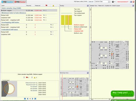
3. Accurate Design Rule Checks
Design rule checks (DRC) are an essential part of the PCB design process. They help ensure that the PCB layout adheres to the specified design rules and manufacturing constraints. PCB Visualizer includes a powerful DRC engine that automatically checks the design for potential issues such as:
- Clearance violations
- Short circuits
- Incorrect trace widths
- Incomplete connections
By running DRC checks throughout the design process, designers can identify and resolve issues early on, reducing the risk of manufacturing defects and costly rework.
4. Seamless Integration with Other Tools
PCB Visualizer seamlessly integrates with other tools in the PCB design ecosystem. It supports various file formats, allowing designers to import and export designs from other software applications. This integration enables a smooth workflow and facilitates collaboration between different teams and stakeholders involved in the PCB design process.
Some of the file formats supported by PCB Visualizer include:
- Gerber files
- ODB++ files
- IPC-2581 files
- Schematic files (e.g., Eagle, KiCad)
PCB Visualizer Workflow
The PCB Visualizer workflow typically involves the following steps:
- Schematic Design: Create a schematic diagram of the electronic circuit using PCB Visualizer or import an existing schematic from another software application.
- Component Placement: Place the components on the PCB layout according to the schematic design. PCB Visualizer provides tools for automatic and manual component placement.
- Routing: Connect the components using traces and vias. PCB Visualizer offers auto-routing capabilities to automate the routing process and manual routing tools for fine-tuning the layout.
- Design Rule Checks: Run DRC checks to ensure that the PCB layout adheres to the specified design rules and manufacturing constraints. PCB Visualizer’s DRC engine identifies potential issues and provides feedback for corrective actions.
- 3D Visualization: Use the 3D visualization feature to inspect the PCB design from different angles and ensure proper component placement and clearance.
- Manufacturing Output: Generate manufacturing files, such as Gerber files or ODB++ files, for PCB fabrication. PCB Visualizer supports various output formats to meet the requirements of different manufacturing processes.

PCB Visualizer Features
PCB Visualizer offers a wide range of features that cater to the needs of PCB designers. Some of the key features include:
1. Multi-Layer PCB Design
PCB Visualizer supports the design of multi-layer PCBs, allowing designers to create complex designs with multiple signal and power layers. The software provides tools for defining layer stackups, specifying layer properties, and managing layer assignments.
2. Auto-Routing
The auto-routing feature in PCB Visualizer automatically routes the connections between components based on the specified design rules. It saves time and effort by automating the routing process, allowing designers to focus on other aspects of the design.
3. Design Rule Checks
PCB Visualizer includes a comprehensive set of design rule checks to ensure the integrity and manufacturability of the PCB design. The DRC engine checks for various issues, such as clearance violations, short circuits, and incorrect trace widths, and provides feedback for corrective actions.
4. 3D Visualization
The 3D visualization feature in PCB Visualizer provides a realistic representation of the PCB design. It allows designers to view the board from different angles, inspect component placement, and identify potential clearance issues. The 3D view helps ensure proper fit and function of the PCB Assembly.
5. Library Management
PCB Visualizer includes a library management system that allows designers to create and manage component libraries. The libraries contain information about the physical and electrical properties of components, making it easier to place and route components accurately.

Frequently Asked Questions (FAQ)
- Is PCB Visualizer suitable for beginners?
Yes, PCB Visualizer is designed to be user-friendly and suitable for both beginners and experienced PCB designers. The software provides a intuitive interface and includes extensive documentation and tutorials to help users get started. - Can PCB Visualizer import designs from other software?
Yes, PCB Visualizer supports various file formats, allowing designers to import designs from other PCB design software applications. It can import schematic files, Gerber files, ODB++ files, and more. - Does PCB Visualizer support multi-layer PCB design?
Yes, PCB Visualizer supports the design of multi-layer PCBs. It provides tools for defining layer stackups, specifying layer properties, and managing layer assignments. - Can I generate manufacturing files using PCB Visualizer?
Yes, PCB Visualizer allows you to generate manufacturing files, such as Gerber files or ODB++ files, for PCB fabrication. The software supports various output formats to meet the requirements of different manufacturing processes. - Is there a limit to the number of components I can place in PCB Visualizer?
No, there is no specific limit to the number of components you can place in PCB Visualizer. However, the performance of the software may be affected by the complexity and size of the design. It is recommended to use appropriate hardware specifications for optimal performance when working with large and complex designs.
Conclusion
PCB Visualizer is a powerful tool that revolutionizes the way PCB designs are created and analyzed. With its user-friendly interface, advanced features, and seamless integration with other tools, PCB Visualizer streamlines the PCB design process and helps engineers and designers create high-quality PCBs efficiently.
By leveraging the benefits of PCB Visualizer, such as improved design efficiency, enhanced visualization capabilities, accurate design rule checks, and seamless integration, designers can reduce the time and effort required to bring their electronic products to market.
Whether you are a beginner or an experienced PCB designer, PCB Visualizer provides the tools and features you need to create professional-grade PCB designs. With its comprehensive library management system, multi-layer PCB support, and powerful auto-routing capabilities, PCB Visualizer is an indispensable tool for anyone involved in PCB design.
So, if you want to take your PCB design skills to the next level and create high-quality PCBs efficiently, consider incorporating PCB Visualizer into your design workflow. With its user-friendly interface and extensive feature set, PCB Visualizer is the ultimate solution for all your PCB design needs.
No responses yet