Introduction to Semiconductor Physics
Band Theory and Energy Gaps
In solid-state physics, the band theory describes the energy levels available to electrons in a solid material. The valence band is the highest range of electron energy levels that are filled with electrons at absolute zero temperature. The conduction band is the lowest range of vacant energy levels. The energy difference between the valence band and the conduction band is known as the band gap or energy gap (Eg).
| Material | Energy Gap (eV) |
|---|---|
| Silicon (Si) | 1.12 |
| Germanium (Ge) | 0.66 |
| Gallium Arsenide (GaAs) | 1.42 |
| Indium Phosphide (InP) | 1.27 |
Intrinsic and Extrinsic Semiconductors
Semiconductors can be classified into two categories based on their purity:
-
Intrinsic semiconductors: These are pure semiconductor materials without any significant dopants or impurities. In intrinsic semiconductors, the number of electrons in the conduction band is equal to the number of holes in the valence band. Examples include ultra-pure silicon and germanium.
-
Extrinsic semiconductors: These are semiconductor materials that have been doped with impurities to modify their electrical properties. Doping introduces additional charge carriers (electrons or holes) into the material. There are two types of extrinsic semiconductors:
- n-type semiconductors: Doped with donor impurities that provide extra electrons.
- p-type semiconductors: Doped with acceptor impurities that create extra holes.
Hole density in Semiconductors
Definition and Concept
Hole density (p) is defined as the number of holes per unit volume in a semiconductor material. It is expressed in units of cm⁻³ (cubic centimeters). In a perfect crystal lattice, all the atoms are bonded together, and there are no missing electrons. However, in reality, thermal energy can cause electrons to break free from their bonds, leaving behind vacant positions called holes.
Relationship with Electron Density
The hole density is closely related to the electron density (n) in a semiconductor. In an intrinsic semiconductor at thermal equilibrium, the electron density and hole density are equal:
n = p = n_i
where n_i is the intrinsic carrier concentration, which depends on the material properties and temperature.
In extrinsic semiconductors, the majority carrier concentration (electrons in n-type or holes in p-type) is much higher than the minority carrier concentration. The product of electron density and hole density remains constant at equilibrium:
n × p = n_i²
Calculation of Hole Density
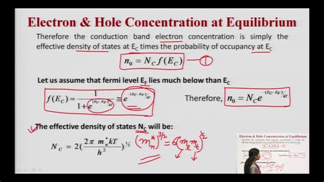
The hole density in a semiconductor can be calculated using the Fermi-Dirac distribution function and the density of states in the valence band. The Fermi-Dirac distribution function f(E) gives the probability of an energy state being occupied by an electron at a given temperature:
f(E) = 1 / (1 + exp((E – E_F) / (k_B × T)))
where E is the energy level, E_F is the Fermi energy, k_B is the Boltzmann constant, and T is the absolute temperature.
The density of states in the valence band N_V(E) represents the number of available energy states per unit volume and energy interval. It depends on the effective mass of holes (m_h*) and the energy gap (Eg):
N_V(E) = (2m_h* / (ħ²π²))³ᐟ² × (E_V – E)^(1/2)
where ħ is the reduced Planck’s constant, and E_V is the top of the valence band.
The hole density can be calculated by integrating the product of the Fermi-Dirac distribution function and the density of states over the entire valence band:
p = ∫ N_V(E) × (1 – f(E)) dE
In practice, the hole density is often determined experimentally through Hall effect measurements or capacitance-voltage profiling techniques.

Factors Affecting Hole Density
Several factors can influence the hole density in a semiconductor material:
-
Temperature: As temperature increases, more electrons gain sufficient thermal energy to break free from their bonds, creating more holes in the valence band. The intrinsic carrier concentration (n_i) increases exponentially with temperature, leading to higher hole densities.
-
Doping concentration: In extrinsic semiconductors, the hole density is primarily determined by the concentration of acceptor dopants (N_A). For a p-type semiconductor, the hole density is approximately equal to the acceptor doping concentration:
p ≈ N_A
-
Impurities and defects: Unintentional impurities and crystallographic defects can introduce additional energy levels within the band gap, affecting the hole density. Deep-level traps can capture and release holes, altering the effective hole concentration.
-
Applied electric field: An external electric field can cause the redistribution of holes within a semiconductor device. In regions where the electric field is strong, such as depletion regions in p-n junctions, the hole density can be significantly different from the equilibrium value.

Applications of Hole Density
Understanding and controlling hole density is essential for various electronic devices and applications:
Solar Cells
In solar cells, the hole density plays a crucial role in the generation and collection of photocurrent. When light is absorbed in a semiconductor, electrons are excited from the valence band to the conduction band, leaving behind holes. The hole density determines the concentration of available charge carriers for electrical conduction. Optimizing the hole density through doping engineering can enhance the efficiency of solar cells.
Light-Emitting Diodes (LEDs)
LEDs rely on the recombination of electrons and holes to emit light. The hole density in the active region of an LED directly affects the luminescence efficiency and brightness. By carefully controlling the hole density through doping and device structure design, high-performance LEDs with desired wavelengths can be achieved.
Bipolar Junction Transistors (BJTs)
BJTs are three-terminal devices that amplify or switch electronic signals. The hole density in the base region of a BJT determines the current gain and switching speed. Proper control of hole density through doping profile engineering is essential for optimizing the performance of BJTs in analog and digital circuits.
Photodetectors
Photodetectors convert optical signals into electrical currents. The hole density in the absorption layer of a photodetector influences its responsivity and detection efficiency. By tailoring the hole density through material selection and doping, photodetectors with high sensitivity and fast response times can be realized.

Frequently Asked Questions (FAQ)
-
What is the difference between hole density and electron density?
Hole density refers to the concentration of vacant positions in the valence band where electrons are missing, while electron density refers to the concentration of electrons in the conduction band. In an intrinsic semiconductor at equilibrium, the hole density and electron density are equal. -
How does temperature affect hole density in semiconductors?
As temperature increases, more electrons gain sufficient thermal energy to break free from their bonds, creating more holes in the valence band. The intrinsic carrier concentration (n_i) increases exponentially with temperature, leading to higher hole densities. -
What is the role of doping in controlling hole density?
Doping is the intentional introduction of impurities into a semiconductor material to modify its electrical properties. In p-type semiconductors, acceptor dopants are added to create extra holes in the valence band. The hole density in a p-type semiconductor is approximately equal to the acceptor doping concentration (N_A). -
How is hole density measured experimentally?
Hole density can be measured using various techniques, including Hall effect measurements and capacitance-voltage profiling. Hall effect measurements involve applying a magnetic field perpendicular to the current flow and measuring the resulting voltage across the sample. Capacitance-voltage profiling uses the voltage-dependent capacitance of a semiconductor device to determine the carrier concentration profile. -
Why is understanding hole density important for electronic devices?
Hole density is a fundamental property that influences the performance and functionality of various electronic devices, such as solar cells, LEDs, bipolar junction transistors, and photodetectors. Controlling hole density through doping engineering and device structure design is crucial for optimizing the efficiency, brightness, current gain, switching speed, and detection capabilities of these devices.
Conclusion
Hole density is a key parameter in semiconductor physics and electrical engineering that describes the concentration of vacant positions in the valence band of a semiconductor material. It is closely related to the electron density and plays a crucial role in the operation of various electronic devices, including solar cells, LEDs, transistors, and photodetectors.
Understanding the factors that influence hole density, such as temperature, doping concentration, impurities, and applied electric fields, is essential for designing and optimizing semiconductor devices. By controlling hole density through material selection, doping engineering, and device structure design, engineers can tailor the performance and functionality of electronic components to meet specific application requirements.
As the field of semiconductor technology continues to advance, the ability to precisely manipulate and characterize hole density will remain crucial for developing high-performance, energy-efficient, and innovative electronic devices that shape our modern world.
No responses yet