Introduction to Peelable Solder Mask
Peelable solder mask, also known as temporary solder mask or peelable mask, is a specialized coating used in printed circuit board (PCB) manufacturing to protect specific areas of the board during the soldering process. Unlike permanent solder masks, which are designed to remain on the PCB throughout its lifetime, peelable solder masks are intended to be removed after soldering is complete. This unique feature allows for Selective Soldering and facilitates various manufacturing processes, such as component assembly, rework, and repair.
What is a Solder Mask?
Before diving into the specifics of peelable solder masks, let’s first understand what a solder mask is and its role in PCB manufacturing. A solder mask, also referred to as a solder resist or solder stop, is a thin layer of polymer that is applied to the surface of a PCB. Its primary purpose is to protect the copper traces and pads from oxidation, prevent solder bridges, and provide electrical insulation.
Solder masks are typically applied using screen printing or photoimaging techniques. They cover the majority of the PCB surface, leaving only the areas that require soldering exposed, such as component pads and connectors. The most common colors for solder masks are green, red, blue, and black, although other colors are available for specific applications or aesthetic purposes.
Advantages of Using a Solder Mask
The use of a solder mask offers several benefits in PCB manufacturing:
- Protection against oxidation: Copper traces and pads on a PCB are susceptible to oxidation when exposed to air, which can lead to poor solderability and reduced electrical performance. By covering these areas with a solder mask, oxidation is prevented, ensuring better solderability and longer shelf life for the PCBs.
- Prevention of solder bridges: During the soldering process, molten solder can sometimes flow between adjacent pads or traces, creating unwanted connections known as solder bridges. These bridges can cause short circuits and lead to device malfunction. Solder masks help prevent solder bridges by providing a barrier between the pads and traces, confining the solder to the intended areas.
- Electrical insulation: Solder masks act as an insulating layer, preventing accidental contact between components and traces. This is particularly important in high-density PCB Designs where the spacing between components and traces is minimal. The insulating properties of the solder mask help maintain the integrity of the electrical connections and reduce the risk of short circuits.
- Improved aesthetics: In addition to their functional benefits, solder masks also contribute to the overall appearance of the PCB. The uniform color and smooth surface provided by the solder mask give the PCB a professional and finished look. This can be especially important for consumer products where aesthetics play a significant role.
What is Peelable Solder Mask?
Peelable solder mask is a specialized type of solder mask that is designed to be easily removed from the PCB surface after the soldering process is complete. Unlike permanent solder masks, which are intended to remain on the board throughout its lifetime, peelable masks serve as a temporary protective layer during specific manufacturing stages.
Composition and Properties of Peelable Solder Masks
Peelable solder masks are typically composed of a base resin, such as polyvinyl alcohol (PVA) or polyvinyl acetate (PVAc), along with various additives that provide the desired properties. These additives may include plasticizers, which improve flexibility and peelability, and fillers, which enhance the mask’s mechanical strength and thermal stability.
The key properties of peelable solder masks include:
- Easy removal: Peelable masks are formulated to be easily stripped from the PCB surface without leaving residue or damaging the underlying components and traces. This is achieved through the use of specific resins and additives that provide a clean and smooth peel.
- Temperature resistance: During the soldering process, peelable masks must withstand high temperatures without degrading or losing their protective properties. Typically, peelable masks are designed to withstand temperatures up to 300°C (572°F) for short durations, making them suitable for most soldering applications.
- Chemical resistance: Peelable masks should be resistant to the chemicals used in the soldering process, such as fluxes and cleaning agents. This ensures that the mask maintains its integrity and protective capabilities throughout the manufacturing process.
- Compatibility with various application methods: Peelable solder masks can be applied using different methods, such as screen printing, spray coating, or dip coating. The mask’s composition is tailored to work well with the chosen application method, ensuring uniform coverage and consistent performance.
Applications of Peelable Solder Masks
Peelable solder masks find use in various stages of PCB manufacturing and assembly, including:
- Selective soldering: In some cases, only specific areas of the PCB need to be soldered, while others must be protected. Peelable masks allow for selective soldering by covering the areas that should not be soldered, leaving only the desired regions exposed. After soldering, the mask is simply peeled off, revealing the protected areas.
- Component assembly: During the component assembly process, peelable masks can be used to protect sensitive areas of the PCB, such as connectors or fine-pitch components. The mask prevents solder bridging and ensures that the components are soldered only at the intended locations.
- Rework and repair: When a PCB requires rework or repair, peelable masks can be applied to protect the surrounding areas while the defective component is removed and replaced. This minimizes the risk of damage to adjacent components and traces during the rework process.
- Conformal coating: In some applications, a conformal coating is applied to the PCB to provide additional protection against moisture, dust, and other environmental factors. Peelable masks can be used to cover areas that should not receive the conformal coating, such as connectors or test points. After the coating is applied and cured, the peelable mask is removed, leaving the desired areas uncoated.

Advantages of Using Peelable Solder Masks
The use of peelable solder masks offers several advantages over traditional permanent solder masks in specific applications:
- Flexibility in design and manufacturing: Peelable masks allow for greater flexibility in PCB design and manufacturing processes. They enable selective soldering, component assembly, and rework without the need for expensive and time-consuming permanent mask modifications.
- Cost-effective for small batches and prototypes: For small production runs or prototype development, using peelable masks can be more cost-effective than creating a dedicated permanent mask. Peelable masks can be easily applied and removed, reducing the time and resources required for mask preparation.
- Simplifies rework and repair processes: When a PCB requires rework or repair, peelable masks simplify the process by protecting the surrounding areas. This reduces the risk of damage to adjacent components and traces, making the rework process faster and more efficient.
- Compatibility with various soldering techniques: Peelable masks are compatible with different soldering techniques, such as wave soldering, selective soldering, and hand soldering. This versatility allows for their use in a wide range of PCB manufacturing and assembly applications.

Challenges and Considerations
While peelable solder masks offer numerous benefits, there are some challenges and considerations to keep in mind when using them:
- Limited durability compared to permanent masks: Peelable masks are designed to be temporary and are not as durable as permanent solder masks. They may not provide the same level of long-term protection against environmental factors, such as moisture and abrasion.
- Potential for residue: If not formulated or applied properly, peelable masks may leave residue on the PCB surface after removal. This residue can interfere with subsequent manufacturing processes or affect the performance of the final product. Proper mask selection and application techniques are crucial to minimize the risk of residue.
- Compatibility with PCB Materials and components: Peelable masks must be compatible with the PCB substrate material and the components used. Some mask formulations may not adhere well to certain substrates or may interact with specific component materials. It is essential to choose a peelable mask that is suitable for the specific PCB design and manufacturing process.
- Need for proper application and removal techniques: To ensure optimal performance, peelable masks must be applied and removed using the appropriate techniques. Improper application can result in uneven coverage or mask damage, while incorrect removal can lead to residue or damage to the PCB. Proper training and adherence to the manufacturer’s guidelines are essential for successful use of peelable masks.
Best Practices for Using Peelable Solder Masks
To maximize the benefits and minimize the challenges associated with peelable solder masks, consider the following best practices:
- Choose the right mask formulation: Select a peelable mask that is compatible with your PCB substrate material, components, and manufacturing processes. Consider factors such as temperature resistance, chemical resistance, and peelability when making your choice.
- Ensure proper mask application: Follow the manufacturer’s guidelines for applying the peelable mask. Use the recommended application method, such as screen printing or spray coating, and ensure that the mask is applied evenly and at the appropriate thickness. Proper application is crucial for achieving optimal protection and peelability.
- Allow sufficient curing time: After application, allow the peelable mask to cure fully before proceeding with the soldering process. Curing times may vary depending on the mask formulation and application thickness. Inadequate curing can result in poor mask performance and difficulty in removal.
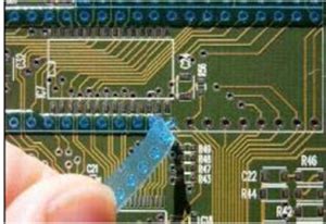
- Use the correct removal technique: When it is time to remove the peelable mask, follow the manufacturer’s instructions carefully. Some masks may require specific removal techniques, such as peeling at a certain angle or using a particular tool. Improper removal can lead to residue or damage to the PCB.
- Inspect the PCB after mask removal: After removing the peelable mask, inspect the PCB thoroughly to ensure that no residue remains and that the protected areas are clean and undamaged. If any issues are identified, address them promptly to avoid potential problems in subsequent manufacturing steps.
- Train personnel on proper use: Ensure that all personnel involved in the application and removal of peelable masks are properly trained. Provide them with the necessary knowledge and skills to handle the masks effectively, minimizing the risk of errors and inconsistencies.
FAQs
- Can peelable solder masks be used on all types of PCBs?
Peelable solder masks can be used on most types of PCBs, including rigid, flexible, and rigid-flex boards. However, it is essential to choose a mask formulation that is compatible with the specific PCB substrate material and components used. - How long do peelable solder masks take to cure?
The curing time for peelable solder masks varies depending on the specific formulation and application thickness. Typically, curing times range from 30 minutes to several hours. It is crucial to follow the manufacturer’s guidelines and allow sufficient curing time to ensure optimal mask performance. - Can peelable solder masks be reused?
No, peelable solder masks are designed for single use only. Once they have been applied, used during the soldering process, and removed, they should be disposed of properly. Attempting to reuse a peelable mask may result in poor performance and potential contamination of the PCB. - What should I do if I notice residue after removing the peelable mask?
If you notice residue on the PCB after removing the peelable mask, it is essential to clean the affected areas thoroughly. Use a compatible cleaning agent and follow the manufacturer’s recommendations for residue removal. If the residue persists or if you notice any damage to the PCB, consult with your PCB Manufacturer or a technical expert for guidance. - Are there any environmental concerns associated with using peelable solder masks?
Peelable solder masks may contain chemicals that can have environmental impacts if not handled and disposed of properly. Always follow the manufacturer’s guidelines for storage, use, and disposal of peelable masks. Adhere to local regulations regarding waste management and disposal to minimize any potential environmental concerns.
Conclusion
Peelable solder masks are a valuable tool in PCB manufacturing, offering flexibility, cost-effectiveness, and simplicity in selective soldering, component assembly, and rework processes. By understanding the composition, properties, and applications of peelable masks, PCB manufacturers can leverage their benefits to improve efficiency and quality in their operations.
However, to ensure the successful use of peelable solder masks, it is crucial to choose the right mask formulation, follow proper application and removal techniques, and adhere to best practices. By doing so, manufacturers can minimize the challenges associated with peelable masks and maximize their potential benefits.
As PCB designs continue to become more complex and demanding, the use of peelable solder masks is likely to grow in importance. By staying informed about the latest developments in peelable mask technology and best practices, PCB manufacturers can remain competitive and deliver high-quality products to their customers.
No responses yet