What is a Carbon Ink PCB?
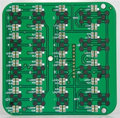
A Carbon Ink PCB, also known as a Carbon-Ink-PCB, is a type of printed circuit board (PCB) that utilizes conductive carbon-based ink instead of traditional copper traces. This innovative technology has gained significant attention in recent years due to its potential for creating low-cost, flexible, and environmentally friendly electronic circuits.
Carbon ink PCBs are manufactured using a printing process, such as screen printing or inkjet printing, to deposit conductive carbon ink onto a substrate material. The substrate can be flexible, like plastic or paper, or rigid, like glass or ceramic. The printed carbon traces form the electrical connections between components, just like the copper traces in a conventional PCB.
Advantages of Carbon Ink PCBs
Carbon ink PCBs offer several advantages over traditional copper-based PCBs:
-
Cost-effectiveness: Carbon ink is generally less expensive than copper, and the printing process is simpler and faster than the etching process used for Copper PCBs. This makes carbon ink PCBs a more cost-effective solution for certain applications.
-
Flexibility: When printed on flexible substrates, carbon ink PCBs can bend and conform to various shapes, making them suitable for wearable electronics, flexible displays, and other applications where flexibility is required.
-
Environmental friendliness: The production of carbon ink PCBs generates less waste and requires fewer harsh chemicals compared to the manufacturing process of traditional PCBs. Additionally, carbon ink is non-toxic and recyclable, making it a more eco-friendly option.
-
Rapid prototyping: The printing process allows for quick and easy prototyping of carbon ink PCBs, enabling faster iteration and development cycles.
Applications of Carbon Ink PCBs
Carbon ink PCBs have found applications in various fields, including:
-
Wearable electronics: The flexibility and lightweight nature of carbon ink PCBs make them ideal for wearable devices, such as smartwatches, fitness trackers, and medical monitoring systems.
-
Internet of Things (IoT): Carbon ink PCBs can be used in IoT devices, such as sensors and smart labels, where low cost and flexibility are important factors.
-
RFID tags: Radio-frequency identification (RFID) tags can be created using carbon ink PCBs, enabling cost-effective and eco-friendly tracking solutions.
-
Disposable electronics: Single-use or disposable electronic devices, such as medical test strips or environmental sensors, can benefit from the low cost and eco-friendliness of carbon ink PCBs.

Limitations of Carbon Ink PCBs
While carbon ink PCBs offer several advantages, they also have some limitations:
-
Lower conductivity: Carbon ink has a higher resistance compared to copper, resulting in lower conductivity. This limits the use of carbon ink PCBs in high-frequency or high-power applications.
-
Limited current carrying capacity: Due to the higher resistance of carbon ink, carbon ink PCBs have a lower current carrying capacity compared to Copper PCBs. This restricts their use in applications that require high current flow.
-
Durability: Carbon ink PCBs may be less durable than copper PCBs, especially when exposed to harsh environmental conditions or mechanical stress.

Manufacturing Process of Carbon Ink PCBs
The manufacturing process of carbon ink PCBs involves several steps:
-
Substrate preparation: The substrate material, such as plastic or paper, is cleaned and treated to ensure proper adhesion of the carbon ink.
-
Carbon ink preparation: The carbon ink is formulated by mixing conductive carbon particles with a binder and solvents to achieve the desired viscosity and electrical properties.
-
Printing: The carbon ink is deposited onto the substrate using a printing method, such as screen printing or inkjet printing. The printing process is controlled to achieve the desired trace thickness and resolution.
-
Curing: After printing, the carbon ink is cured using heat or ultraviolet (UV) light to evaporate the solvents and solidify the traces.
-
Component assembly: Electronic components are placed and attached to the carbon ink PCB using conductive adhesives or other suitable methods.
-
Encapsulation (optional): In some cases, the carbon ink PCB may be encapsulated or coated with a protective layer to enhance its durability and resistance to environmental factors.
Comparison with Traditional Copper PCBs
The following table compares the key characteristics of carbon ink PCBs and traditional copper PCBs:
| Characteristic | Carbon Ink PCB | Copper PCB |
|---|---|---|
| Conductivity | Lower | Higher |
| Current capacity | Lower | Higher |
| Flexibility | High | Low |
| Cost | Lower | Higher |
| Environmental impact | Lower | Higher |
| Durability | Lower | Higher |
| High-frequency performance | Limited | Better |
Future Trends and Research
The field of carbon ink PCBs is continually evolving, with ongoing research and development focused on improving their performance and expanding their applications. Some of the key areas of interest include:
-
Enhancing conductivity: Researchers are working on developing new carbon ink formulations and processing techniques to increase the conductivity of carbon ink PCBs, bringing them closer to the performance of copper PCBs.
-
Hybrid PCBs: Combining carbon ink with other conductive materials, such as silver nanoparticles or metal mesh, to create hybrid PCBs that offer the benefits of both technologies.
-
3D printing: Exploring the use of 3D printing techniques to create complex, three-dimensional carbon ink PCB Structures for advanced electronics applications.
-
Sustainable materials: Investigating the use of biodegradable and renewable substrates, such as paper or bioplastics, to further enhance the eco-friendliness of carbon ink PCBs.
-
Advanced applications: Expanding the use of carbon ink PCBs in emerging fields, such as bioelectronics, energy storage, and smart packaging.
Frequently Asked Questions (FAQ)
-
Q: Can carbon ink PCBs replace copper PCBs in all applications?
A: No, carbon ink PCBs are not suitable for all applications due to their lower conductivity and current carrying capacity compared to copper PCBs. They are best suited for low-power, low-frequency applications where flexibility and cost are important factors. -
Q: Are carbon ink PCBs as durable as copper PCBs?
A: Carbon ink PCBs are generally less durable than copper PCBs, especially when exposed to harsh environmental conditions or mechanical stress. However, encapsulation or protective coatings can be applied to enhance their durability. -
Q: Can carbon ink PCBs be recycled?
A: Yes, carbon ink PCBs are recyclable, as the carbon ink can be separated from the substrate material. This makes them a more environmentally friendly option compared to traditional PCBs. -
Q: What is the resolution of carbon ink PCBs?
A: The resolution of carbon ink PCBs depends on the printing method used. Screen printing can typically achieve a resolution of around 100 μm, while inkjet printing can achieve higher resolutions, down to 50 μm or less. -
Q: Are carbon ink PCBs suitable for high-frequency applications?
A: Carbon ink PCBs have limited performance in high-frequency applications due to their lower conductivity compared to copper PCBs. They are better suited for low-frequency applications, typically below a few MHz.
Conclusion
Carbon ink PCBs represent a promising alternative to traditional copper PCBs, offering advantages such as cost-effectiveness, flexibility, and environmental friendliness. While they have limitations in terms of conductivity and current carrying capacity, they have found applications in various fields, including wearable electronics, IoT devices, and disposable electronics.
As research and development continue, it is expected that the performance and applications of carbon ink PCBs will expand, making them an increasingly attractive option for the electronics industry. With the growing demand for flexible, low-cost, and eco-friendly electronics, carbon ink PCBs are poised to play a significant role in shaping the future of printed circuit board technology.
No responses yet