Introduction to AOI in PCB Manufacturing
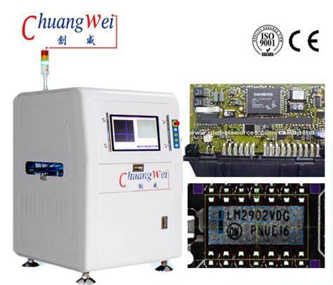
Automated Optical Inspection (AOI) is a critical quality control process used in the manufacturing of Printed Circuit Boards (PCBs). AOI systems use high-resolution cameras and advanced image processing algorithms to inspect PCBs for defects, ensuring that they meet the required quality standards before being assembled into electronic devices.
In this article, we will explore the importance of AOI in PCB manufacturing, how it works, its benefits, and the different types of AOI systems used in the industry.
What is a Printed Circuit Board (PCB)?
A Printed Circuit Board (PCB) is a thin board made of fiberglass or composite material that is used to mechanically support and electrically connect electronic components using conductive pathways, tracks, or signal traces etched from copper sheets laminated onto a non-conductive substrate.
PCBs are the foundation of modern electronics and are used in a wide range of applications, from consumer electronics to aerospace and medical devices. They provide a reliable and efficient means of connecting electronic components, allowing for compact and complex circuits to be designed and manufactured.
Types of PCBs
There are several types of PCBs, each with its own unique characteristics and applications. The most common types of PCBs include:
-
Single-sided PCBs: These PCBs have conductive traces on only one side of the board. They are the simplest and most cost-effective type of PCB, suitable for low-complexity circuits.
-
Double-sided PCBs: These PCBs have conductive traces on both sides of the board, allowing for more complex circuits and higher component density. They are commonly used in consumer electronics and telecommunications equipment.
-
Multi-layer PCBs: These PCBs consist of multiple layers of conductive traces separated by insulating layers. They offer the highest component density and are used in advanced applications such as high-speed computing and aerospace systems.
-
Flexible PCBs: These PCBs are made from flexible materials, allowing them to bend and conform to various shapes. They are used in applications where space is limited or where the PCB needs to flex during operation, such as in wearable devices and automotive electronics.
-
Rigid-Flex PCBs: These PCBs combine the benefits of rigid and flexible PCBs, with rigid sections for mounting components and flexible sections for connecting them. They are used in applications that require both high component density and flexibility, such as in medical devices and military equipment.

The Importance of Quality Control in PCB Manufacturing
Quality control is essential in PCB manufacturing to ensure that the boards meet the required specifications and perform reliably in their intended applications. Defects in PCBs can lead to malfunctions, reduced performance, and even complete failure of the electronic devices they are used in.
Some common PCB defects include:
- Short circuits
- Open circuits
- Incorrect component placement
- Solder bridging
- Insufficient solder
- Damaged components
These defects can arise from various factors, such as design flaws, manufacturing process errors, and material defects. Detecting and correcting these defects early in the manufacturing process is crucial to avoid costly rework and delays in product delivery.
Traditional manual inspection methods are time-consuming, labor-intensive, and prone to human error. As PCBs become more complex and miniaturized, manual inspection becomes increasingly difficult and inefficient. This is where Automated Optical Inspection (AOI) comes into play.

How Does AOI Work in PCB Inspection?
AOI systems use high-resolution cameras and advanced image processing algorithms to inspect PCBs for defects. The process involves the following steps:
-
Image Acquisition: The AOI system captures high-resolution images of the PCB from various angles using multiple cameras. These images are typically captured under specific lighting conditions to enhance the visibility of defects.
-
Image Processing: The captured images are then processed using advanced algorithms to identify and locate defects. These algorithms compare the captured images to a reference image of a known good PCB, looking for any deviations or anomalies.
-
Defect Detection: The AOI system flags any detected defects and classifies them based on their type and severity. Common defect types include solder bridges, open circuits, short circuits, and component placement errors.
-
Defect Verification: The flagged defects are then verified by a human operator to confirm their presence and determine the appropriate corrective action. Some AOI systems include automated defect verification capabilities to reduce the need for human intervention.
-
Reporting: The AOI system generates a detailed report of the inspection results, including the types and locations of the detected defects. This report is used to track the quality of the PCBs and identify areas for process improvement.
Advantages of AOI in PCB Manufacturing
AOI offers several advantages over traditional manual inspection methods in PCB manufacturing:
-
Increased Efficiency: AOI systems can inspect PCBs much faster than human operators, allowing for higher throughput and reduced inspection times.
-
Improved Accuracy: AOI systems are not subject to human fatigue or error, ensuring consistent and reliable defect detection.
-
Early Defect Detection: AOI can detect defects early in the manufacturing process, allowing for timely corrective action and reducing the risk of costly rework and scrap.
-
Reduced Labor Costs: AOI systems can reduce the need for manual inspection, leading to lower labor costs and increased productivity.
-
Traceability: AOI systems generate detailed inspection reports that can be used to track the quality of PCBs and identify areas for process improvement.

Types of AOI Systems Used in PCB Manufacturing
There are several types of AOI systems used in PCB manufacturing, each with its own unique capabilities and applications:
2D AOI Systems
2D AOI systems use a single camera to capture images of the PCB from a fixed angle. They are typically used for inspecting the surface of the PCB, detecting defects such as solder bridges, open circuits, and component placement errors.
Advantages of 2D AOI systems include:
- Lower cost compared to 3D AOI systems
- Faster inspection times
- Suitable for inspecting simple PCBs with flat surfaces
Limitations of 2D AOI systems include:
- Limited ability to detect defects on non-planar surfaces
- Difficulty detecting defects in hard-to-reach areas, such as under components
3D AOI Systems
3D AOI systems use multiple cameras or laser scanners to capture 3D images of the PCB. They can inspect both the surface and the height of the PCB, detecting defects such as insufficient solder, lifted components, and warpage.
Advantages of 3D AOI systems include:
- Ability to detect defects on non-planar surfaces and in hard-to-reach areas
- Higher accuracy and reliability compared to 2D AOI systems
- Suitable for inspecting complex PCBs with high component density
Limitations of 3D AOI systems include:
- Higher cost compared to 2D AOI systems
- Slower inspection times due to the need for multiple image captures
Inline AOI Systems
Inline AOI systems are integrated into the PCB manufacturing line, inspecting the PCBs immediately after each process step. They are used to detect defects as soon as they occur, allowing for timely corrective action and reducing the risk of scrap and rework.
Advantages of inline AOI systems include:
- Early defect detection, reducing the risk of scrap and rework
- Seamless integration into the manufacturing process
- Real-time process monitoring and control
Limitations of inline AOI systems include:
- Higher initial investment cost compared to standalone AOI systems
- Potential for bottlenecks in the manufacturing line if the AOI system is slower than the other processes
Standalone AOI Systems
Standalone AOI systems are used for offline inspection of PCBs, typically after the manufacturing process is complete. They are used for final quality control and to inspect PCBs that have been returned for rework or repair.
Advantages of standalone AOI systems include:
- Flexibility in scheduling inspections
- Ability to inspect PCBs from multiple manufacturing lines
- Lower initial investment cost compared to inline AOI systems
Limitations of standalone AOI systems include:
- Later defect detection compared to inline AOI systems
- Potential for increased scrap and rework if defects are not caught early in the manufacturing process
Best Practices for Implementing AOI in PCB Manufacturing
To maximize the benefits of AOI in PCB manufacturing, it is important to follow best practices for implementation and operation:
-
Select the Right AOI System: Choose an AOI system that is suitable for your specific PCB manufacturing needs, considering factors such as PCB complexity, component density, and inspection requirements.
-
Develop Robust Inspection Programs: Develop inspection programs that are tailored to your specific PCB designs and manufacturing processes. This includes selecting the appropriate lighting conditions, camera angles, and image processing algorithms.
-
Establish Clear Defect Criteria: Establish clear criteria for what constitutes a defect, based on industry standards and customer requirements. This helps ensure consistent and reliable defect detection.
-
Train Operators: Provide thorough training to AOI system operators to ensure they are proficient in using the system and interpreting the inspection results.
-
Regularly Calibrate and Maintain Equipment: Regularly calibrate and maintain the AOI system to ensure accurate and reliable performance. This includes cleaning the cameras and lighting system, updating software, and replacing worn or damaged components.
-
Integrate with Other Quality Control Processes: Integrate the AOI system with other quality control processes, such as in-circuit testing and functional testing, to provide a comprehensive quality assurance program.
-
Continuously Monitor and Improve: Continuously monitor the performance of the AOI system and the quality of the PCBs it inspects. Use the data generated by the system to identify areas for process improvement and implement corrective actions as needed.
Frequently Asked Questions (FAQ)
-
What is the difference between AOI and visual inspection?
AOI is an automated process that uses high-resolution cameras and advanced image processing algorithms to inspect PCBs for defects, while visual inspection is a manual process performed by human operators. AOI is faster, more accurate, and more consistent than visual inspection, but it requires a higher initial investment in equipment and training. -
Can AOI detect all types of PCB defects?
While AOI is highly effective at detecting a wide range of PCB defects, it may not be able to detect all types of defects, particularly those that are not visible on the surface of the PCB. Some defects, such as internal shorts or opens, may require additional testing methods, such as in-circuit testing or X-ray inspection. -
How much does an AOI system cost?
The cost of an AOI system can vary widely depending on factors such as the type of system (2D or 3D), the inspection capabilities, and the level of automation. Basic 2D AOI systems can cost around $50,000, while advanced 3D AOI systems with automated handling and reporting capabilities can cost upwards of $500,000. -
How long does it take to inspect a PCB using AOI?
The inspection time for a PCB using AOI can vary depending on the size and complexity of the board, as well as the type of AOI system being used. Typically, a 2D AOI system can inspect a simple PCB in a few seconds, while a 3D AOI system may take several minutes to inspect a complex, high-density PCB. -
Can AOI be used for other applications besides PCB inspection?
Yes, AOI technology can be adapted for use in a wide range of applications beyond PCB inspection, such as in the manufacturing of semiconductors, displays, and medical devices. AOI can be used to inspect any product or component that requires high-precision, high-speed visual inspection for defects or anomalies.
Conclusion
Automated Optical Inspection (AOI) is a critical quality control process in PCB manufacturing that uses high-resolution cameras and advanced image processing algorithms to inspect PCBs for defects. AOI offers several advantages over traditional manual inspection methods, including increased efficiency, improved accuracy, early defect detection, reduced labor costs, and traceability.
There are several types of AOI systems used in PCB manufacturing, including 2D AOI, 3D AOI, inline AOI, and standalone AOI. Each type has its own unique capabilities and limitations, and the choice of system depends on factors such as PCB complexity, component density, and inspection requirements.
To maximize the benefits of AOI in PCB manufacturing, it is important to follow best practices for implementation and operation, such as selecting the right AOI system, developing robust inspection programs, establishing clear defect criteria, training operators, regularly calibrating and maintaining equipment, integrating with other quality control processes, and continuously monitoring and improving.
As PCBs continue to become more complex and miniaturized, the importance of AOI in ensuring their quality and reliability will only continue to grow. By investing in AOI technology and following best practices for its implementation and operation, PCB Manufacturers can improve their quality control processes, reduce costs, and deliver higher-quality products to their customers.
No responses yet