Key Features of PCB Design software
Modern PCB design software offer a wide range of features and capabilities to streamline the design process. Some of the essential features include:
Schematic Capture
Schematic capture is the process of creating a graphical representation of the electrical connections and components in a circuit. PCB design software provide schematic editors with extensive libraries of symbols representing various electronic components. Engineers can place these symbols on the schematic and create connections between them using wires or nets.
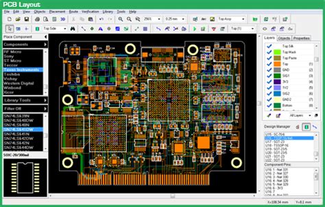
Board Layout
Once the schematic is complete, PCB design software allow engineers to create the physical layout of the circuit board. This involves placing components on the board and routing the connections between them using copper traces. The software provides tools for manual and automatic routing, layer stackup definition, and design rule checking (DRC) to ensure the layout meets manufacturing constraints.
3D Visualization
Many PCB design software packages now offer 3D visualization capabilities, allowing engineers to view their designs in a three-dimensional space. This feature helps in identifying potential mechanical interferences, optimizing component placement, and ensuring proper clearances.
Simulation and Analysis
Advanced PCB design software integrate simulation and analysis tools to help engineers optimize their designs for signal integrity, power integrity, and electromagnetic compatibility (EMC). These tools can perform signal integrity simulations, power delivery network analysis, and electromagnetic interference (EMI) analysis to identify and resolve potential issues before the board is manufactured.
Library Management
PCB design software provide tools for managing libraries of components, footprints, and symbols. These libraries can be customized and shared among team members to ensure consistency and reduce design time.
Popular PCB Design Software
There are several popular PCB design software packages available in the market, each with its own strengths and target audience. Some of the widely used PCB design software include:
| Software | Vendor | Target Audience |
|---|---|---|
| Altium Designer | Altium | Professional engineers and large enterprises |
| OrCAD | Cadence Design Systems | Professional engineers and large enterprises |
| EAGLE | Autodesk | Hobbyists, students, and small businesses |
| KiCad | Open-source | Hobbyists, students, and small businesses |
| PADS | Mentor Graphics | Professional engineers and large enterprises |
Altium Designer
Altium Designer is a high-end PCB design software package used by professional engineers and large enterprises. It offers a comprehensive set of features for schematic capture, board layout, 3D visualization, and simulation. Altium Designer is known for its powerful routing capabilities, extensive component libraries, and integration with mechanical CAD (MCAD) software.
OrCAD
OrCAD, developed by Cadence Design Systems, is another popular PCB design software suite used by professional engineers and large enterprises. It consists of several modules, including OrCAD Capture for schematic design, OrCAD PCB Editor for board layout, and OrCAD PSpice for circuit simulation. OrCAD is known for its robust design rule checking and simulation capabilities.
EAGLE
EAGLE (Easily Applicable Graphical Layout Editor) is a PCB design software package developed by Autodesk. It is popular among hobbyists, students, and small businesses due to its user-friendly interface and affordable pricing. EAGLE offers schematic capture, board layout, and autorouting features, along with an extensive library of components.
KiCad
KiCad is an Open-source PCB design software suite that has gained popularity in recent years. It offers schematic capture, board layout, and 3D visualization capabilities. KiCad is known for its active user community, which contributes to its development and provides support through forums and tutorials.
PADS
PADS, developed by Mentor Graphics (now part of Siemens), is a PCB design software package targeted towards professional engineers and large enterprises. It offers schematic capture, board layout, and simulation features, along with strong design rule checking and constraint management capabilities.

Choosing the Right PCB Design Software
When selecting a PCB design software package, engineers should consider several factors:
Functionality
The software should provide all the necessary features for schematic capture, board layout, and simulation to meet the specific requirements of the project. Consider the complexity of the designs, the need for advanced simulation capabilities, and the level of automation required.
Ease of Use
The user interface and workflow of the software should be intuitive and efficient. Look for software with good documentation, tutorials, and user community support to help in learning and troubleshooting.
Integration
If the PCB design needs to be integrated with mechanical design or other CAD tools, consider software that offers seamless integration capabilities. This can streamline the design process and ensure compatibility between electrical and mechanical aspects of the product.
Scalability
Choose a software package that can scale with the growth of the project or organization. Consider the ability to handle larger and more complex designs, collaborate with team members, and manage design data effectively.
Cost
PCB design software packages vary in pricing, ranging from free open-source options to high-end commercial solutions. Consider the budget constraints and the long-term cost of ownership, including maintenance, upgrades, and support.

Best Practices for Using PCB Design Software
To effectively use PCB design software and create high-quality PCB designs, engineers should follow some best practices:
Start with a Clear Schematic
Ensure that the schematic diagram is well-organized, properly labeled, and follows good design practices. Use hierarchical design techniques to manage complexity and improve readability.
Define Design Rules Early
Establish the design rules and constraints early in the design process. This includes specifying the layer stackup, trace widths, clearances, and manufacturing constraints. Consistently apply these rules throughout the design.
Use a Consistent Naming Convention
Adopt a consistent naming convention for components, nets, and layers. This helps in navigating the design, collaborating with team members, and generating accurate manufacturing files.
Optimize Component Placement
Place components strategically on the board to minimize trace lengths, reduce signal interference, and improve manufacturability. Consider the mechanical constraints and the thermal requirements of the components.
Route Carefully
Use appropriate routing techniques, such as avoiding sharp angles, minimizing vias, and providing proper termination for high-speed signals. Follow the recommended trace widths and spacing for the specific signal types and frequencies.
Perform Design Rule Checks
Regularly run design rule checks (DRC) to identify and resolve any violations of the established design rules. This helps in catching errors early and ensuring the design is manufacturable.
Collaborate and Version Control
Use version control and collaboration tools provided by the PCB design software to manage design changes, track revisions, and work effectively with team members.

FAQ
What is the difference between schematic capture and board layout?
Schematic capture involves creating a graphical representation of the electrical connections and components in a circuit, while board layout involves placing those components on a physical board and routing the connections between them using copper traces.
Can I customize the component libraries in PCB design software?
Yes, most PCB design software allow users to create and customize component libraries. This enables engineers to add new components, modify existing ones, and ensure consistency across designs.
What is the purpose of design rule checking (DRC)?
Design rule checking (DRC) is a feature in PCB design software that verifies the design against a set of predefined rules and constraints. It helps in identifying any violations, such as insufficient clearances, incorrect trace widths, or missing connections, ensuring the design is error-free and manufacturable.
How do I choose the right layer stackup for my PCB design?
The choice of layer stackup depends on several factors, including the complexity of the design, the signal integrity requirements, and the manufacturing constraints. Consult with the PCB manufacturer and consider the specific needs of the project to determine the appropriate layer stackup.
Can I import CAD files from other software into PCB design software?
Most PCB design software support importing CAD files from other software, such as mechanical CAD (MCAD) tools. This allows for seamless integration between electrical and mechanical design, ensuring proper fit and alignment of components on the board.
Conclusion
PCB design software are essential tools for creating high-quality and reliable printed circuit boards. They offer a wide range of features and capabilities to streamline the design process, from schematic capture and board layout to simulation and analysis. When selecting a PCB design software package, engineers should consider factors such as functionality, ease of use, integration, scalability, and cost. By following best practices and leveraging the capabilities of these software tools, engineers can efficiently design complex PCBs that meet the requirements of their projects.
No responses yet