What is PCB Visualization?
PCB Visualization refers to the various methods and tools used to graphically represent printed circuit boards (PCBs) during the design, manufacturing, and assembly processes. By visualizing PCBs in 2D and 3D, engineers and other stakeholders can more easily understand the board layout, identify potential issues, and streamline the entire PCB development workflow.
Benefits of PCB Visualization
Implementing PCB visualization techniques offers several key advantages:
-
Improved Communication: Visual representations of PCBs make it easier for team members from different departments to understand and discuss the board design.
-
Faster Issue Detection: 3D models and detailed 2D layouts help identify design flaws, component placement issues, and potential manufacturing challenges early in the process.
-
Enhanced Collaboration: Sharing visual PCB data facilitates collaboration between design teams, manufacturers, and clients.
-
Reduced Time-to-Market: By catching and resolving issues early, PCB visualization helps accelerate the development process and brings products to market faster.
PCB Visualization Techniques
There are several methods for visualizing PCBs, each with its own strengths and applications:
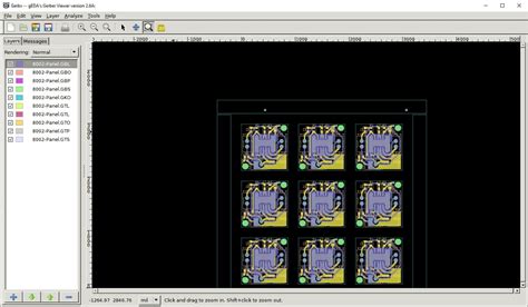
2D PCB Layout Visualization
2D PCB layout visualization is the foundation of the PCB design process. It involves creating a flat representation of the board, showing the placement of components, traces, and other features. Key aspects of 2D PCB layout visualization include:
- Layer Stackup: A visual representation of the PCB’s layers, including copper, insulation, and solder mask layers.
- Component Placement: Showing the location and orientation of components on the board.
- Trace Routing: Displaying the paths of the electrical traces connecting components.
- Design Rule Checking (DRC): Visually highlighting design rule violations, such as insufficient clearances or trace widths.
3D PCB Visualization
3D PCB visualization takes PCB representation to the next level by creating a three-dimensional model of the board. This allows for a more realistic and intuitive understanding of the PCB design. 3D PCB visualization includes:
- Board and Component Models: Realistic 3D representations of the PCB and its components.
- Mechanical Fit Checking: Verifying that components fit properly and do not interfere with each other or the enclosure.
- Clearance Checking: Ensuring adequate space between components and other board features.
- Thermal Analysis: Visualizing heat distribution across the PCB to identify potential thermal issues.
PCB Assembly Visualization
PCB assembly visualization focuses on the manufacturing and assembly aspects of PCB production. It helps manufacturers optimize the assembly process and catch potential issues before they occur. PCB assembly visualization includes:
- Assembly Drawing Creation: Generating visual instructions for PCB assembly, including component placement and orientation.
- Pick-and-Place Machine Programming: Creating visual data to guide automated component placement machines.
- Solder Paste Stencil Design: Designing and visualizing solder paste stencils for optimal solder paste application.

PCB Visualization Tools
There are numerous software tools available for PCB visualization, ranging from simple 2D layout editors to advanced 3D modeling and simulation packages. Some popular PCB visualization tools include:
| Tool | 2D Layout | 3D Modeling | Thermal Analysis | DRC | Manufacturer Support |
|---|---|---|---|---|---|
| Altium Designer | ✓ | ✓ | ✓ | ✓ | ✓ |
| KiCad | ✓ | ✓ | ✓ | ||
| Autodesk Eagle | ✓ | ✓ | ✓ | ✓ | |
| Cadence OrCAD | ✓ | ✓ | ✓ | ✓ | ✓ |
| Zuken CR-8000 | ✓ | ✓ | ✓ | ✓ | ✓ |
Integrating PCB Visualization into the Business Process
To fully leverage the benefits of PCB visualization, it is essential to integrate visualization techniques and tools into the entire PCB development process. This involves:
-
Design Phase: Use 2D layout and 3D modeling tools to create and refine the PCB design, catching issues early and optimizing the layout.
-
Collaboration: Share visual PCB data with team members, manufacturers, and clients to facilitate communication and collaboration.
-
Manufacturing Preparation: Utilize PCB assembly visualization to create assembly drawings, program pick-and-place machines, and design solder paste stencils.
-
Quality Control: Employ visual inspection techniques to verify the manufactured PCBs against the original design.
By integrating PCB visualization throughout the business process, companies can streamline their PCB development efforts, reduce errors, and bring high-quality products to market more quickly.

Best Practices for Effective PCB Visualization
To maximize the benefits of PCB visualization, consider the following best practices:
-
Choose the Right Tools: Select PCB visualization software that meets your specific needs and integrates well with your existing design and manufacturing processes.
-
Establish Design Standards: Develop and adhere to a set of design standards to ensure consistency and clarity in your visual PCB representations.
-
Leverage Automation: Utilize automated features in your PCB visualization tools, such as design rule checking and 3D model generation, to save time and reduce errors.
-
Collaborate Effectively: Establish clear communication channels and protocols for sharing visual PCB data with team members and stakeholders.
-
Continuously Improve: Regularly review and optimize your PCB visualization practices based on feedback and lessons learned from previous projects.

The Future of PCB Visualization
As technology advances, PCB visualization techniques and tools will continue to evolve. Some emerging trends and future developments in PCB visualization include:
- Augmented and Virtual Reality (AR/VR): Integrating AR and VR technologies with PCB visualization to create immersive, interactive experiences for design and collaboration.
- AI-Assisted Design: Leveraging artificial intelligence and machine learning to optimize PCB layouts and catch design issues automatically.
- Cloud-Based Collaboration: Moving PCB visualization and collaboration tools to the cloud, enabling real-time, global collaboration and data access.
- Integration with PLM Systems: Integrating PCB visualization data with product lifecycle management (PLM) systems to provide a holistic view of the product development process.
By staying up-to-date with these emerging trends and technologies, companies can position themselves at the forefront of PCB development and maintain a competitive edge in their industry.
Frequently Asked Questions (FAQ)
-
What is the difference between 2D and 3D PCB visualization?
2D PCB visualization focuses on the flat representation of the board layout, showing components, traces, and layers. 3D PCB visualization creates a three-dimensional model of the board, allowing for a more realistic and intuitive understanding of the design, including mechanical fit and clearance checking. -
How does PCB visualization help with collaboration?
PCB visualization makes it easier for team members from different departments, as well as external stakeholders like manufacturers and clients, to understand and discuss the board design. By sharing visual PCB data, collaboration becomes more efficient and effective. -
What are some common PCB visualization software tools?
Some popular PCB visualization tools include Altium Designer, KiCad, Autodesk Eagle, Cadence OrCAD, and Zuken CR-8000. These tools offer a range of features for 2D layout, 3D modeling, thermal analysis, and design rule checking. -
How can I integrate PCB visualization into my company’s business process?
To integrate PCB visualization into your business process, use visualization tools throughout the design phase, share visual data to facilitate collaboration, utilize assembly visualization for manufacturing preparation, and employ visual inspection techniques for quality control. -
What are some emerging trends in PCB visualization?
Some emerging trends in PCB visualization include the use of augmented and virtual reality (AR/VR) for immersive design experiences, AI-assisted design for layout optimization, cloud-based collaboration tools, and integration with product lifecycle management (PLM) systems.
By understanding and implementing effective PCB visualization techniques, companies can streamline their PCB development process, reduce errors, and ultimately bring better products to market faster. As technology continues to advance, staying current with the latest visualization tools and trends will be essential for success in the competitive world of PCB design and manufacturing.
No responses yet