What are PCB tolerances and Why Do They Matter?
In the world of printed circuit board (PCB) manufacturing, tolerances play a crucial role in ensuring the quality, reliability, and functionality of the final product. PCB Tolerances refer to the acceptable range of variation in the dimensions, spacing, and alignment of the various components and features on a PCB. These tolerances are essential because they account for the inherent limitations and variability in the manufacturing process, materials, and equipment used to produce PCBs.
Maintaining tight tolerances is critical for several reasons:
-
Functionality: Proper tolerances ensure that components fit correctly on the PCB and that the board functions as intended. If tolerances are not met, components may not align properly, leading to poor connections, short circuits, or other issues that can compromise the performance of the PCB.
-
Reliability: PCBs that are manufactured within the specified tolerances are more likely to be reliable and have a longer lifespan. Inconsistencies in the manufacturing process can lead to stress on components, trace breakage, or other defects that can cause premature failure of the PCB.
-
Compatibility: Adhering to industry-standard tolerances ensures that PCBs are compatible with other components and systems. This is particularly important when designing boards that need to interface with existing equipment or when working with multiple vendors for different parts of a project.
-
Cost: While tighter tolerances may increase the manufacturing cost of a PCB, they can ultimately save money by reducing the likelihood of defects, rework, and field failures. Striking the right balance between cost and quality is essential for any successful PCB project.
Types of PCB Tolerances
There are several types of tolerances that need to be considered when designing and manufacturing PCBs. Some of the most critical tolerances include:
-
Dimensional Tolerances: These tolerances refer to the acceptable variation in the physical dimensions of the PCB, such as length, width, and thickness. Dimensional tolerances also encompass the size and location of holes, slots, and other features on the board.
-
Copper Thickness Tolerances: The thickness of the copper traces on a PCB can vary depending on the manufacturing process and the specified requirements. Copper thickness tolerances ensure that the traces have the appropriate current-carrying capacity and impedance characteristics.
-
Spacing Tolerances: These tolerances define the minimum acceptable distances between various features on the PCB, such as traces, pads, and components. Maintaining proper spacing is essential for preventing short circuits, electromagnetic interference (EMI), and other issues that can arise from components being too close together.
-
Alignment Tolerances: Alignment tolerances refer to the acceptable variation in the position of components, holes, and other features relative to each other and to the edges of the PCB. Proper alignment is critical for ensuring that components fit correctly and that the board functions as intended.
-
Soldermask and Silkscreen Tolerances: Soldermask and silkscreen are the protective coatings and markings applied to the surface of a PCB. Tolerances for these features ensure that they are correctly aligned with the underlying copper traces and pads and that they do not interfere with the function of the board.
Factors Affecting PCB Tolerances
Several factors can influence the tolerances that can be achieved in PCB manufacturing. Understanding these factors is essential for designing boards that can be manufactured reliably and cost-effectively.
Materials
The materials used in PCB manufacturing, such as the substrate, copper foil, and soldermask, can have a significant impact on the achievable tolerances. Different materials have varying properties, such as thermal expansion, flexural strength, and dimensional stability, which can affect the precision and consistency of the manufacturing process.
For example, FR-4, a common PCB substrate material, has a relatively high coefficient of thermal expansion (CTE), which means that it can expand and contract significantly with changes in temperature. This can lead to challenges in maintaining tight tolerances, particularly for larger boards or those with fine-pitch components.
Manufacturing Process
The manufacturing process used to produce PCBs can also have a significant impact on the achievable tolerances. Different processes, such as etching, drilling, and plating, have their own limitations and variability that can affect the precision and consistency of the final product.
For instance, the etching process used to create copper traces on a PCB can be influenced by factors such as the etchant chemistry, temperature, and agitation. Variations in these factors can lead to inconsistencies in the width and thickness of the traces, which can impact the electrical performance and reliability of the board.
Equipment
The equipment used in PCB manufacturing, such as CNC machines, drills, and plating equipment, can also influence the achievable tolerances. The accuracy, repeatability, and maintenance of this equipment can have a direct impact on the precision and consistency of the manufacturing process.
For example, worn or poorly maintained drill bits can lead to inconsistencies in hole size and location, while outdated or low-quality imaging equipment can result in misaligned or blurred soldermask and silkscreen features.
Design Complexity
The complexity of the PCB design can also have a significant impact on the achievable tolerances. Boards with high component density, fine-pitch traces, or complex geometries may require tighter tolerances to ensure proper functionality and reliability.
In general, more complex designs will require more advanced manufacturing processes and equipment, which can increase the cost and lead time of the project. Designers need to balance the complexity of the board with the capabilities of the manufacturing process and the project budget and timeline.

Industry Standards for PCB Tolerances
To ensure consistency and compatibility across the PCB industry, several standards organizations have developed guidelines and specifications for PCB tolerances. These standards provide a common language and set of expectations for designers, manufacturers, and end-users of PCBs.
IPC Standards
The Association Connecting Electronics Industries (IPC) is the most widely recognized standards organization for the PCB industry. IPC standards cover a wide range of topics, including design, manufacturing, assembly, and testing of PCBs.
Some of the most relevant IPC standards for PCB tolerances include:
- IPC-6012: This standard defines the qualification and performance specifications for rigid printed boards, including tolerances for dimensions, hole size, and placement accuracy.
- IPC-6013: This standard provides qualification and performance specifications for flexible printed boards, including tolerances for conductor width and spacing, cover layer thickness, and overall board thickness.
- IPC-2221: This standard provides generic requirements for the design of printed boards and printed board assemblies, including guidelines for conductor width and spacing, hole size and placement, and soldermask and silkscreen features.
- IPC-7351: This standard provides guidelines for land pattern geometries used for surface-mount and through-hole components, including tolerances for pad size, shape, and spacing.
Other Standards
In addition to IPC standards, there are several other organizations that provide guidelines and specifications for PCB tolerances, including:
- JEDEC (Joint Electron Device Engineering Council): JEDEC standards cover a wide range of topics related to semiconductor devices and packaging, including PCB tolerances for land patterns and component footprints.
- Mil-Spec (Military Specification): Mil-spec standards are developed by the United States Department of Defense and provide requirements for PCBs used in military and aerospace applications. These standards often have more stringent tolerance requirements than commercial standards to ensure reliability in harsh environments.
- ISO (International Organization for Standardization): ISO standards cover a wide range of industries and topics, including some related to PCB manufacturing and tolerances.
Table 1: Common IPC Tolerances for Rigid PCBs (IPC-6012)
| Feature | Tolerance (mm) |
|————————————–|—————-|
| Board thickness | ±10% |
| Board outline | ±0.15 |
| Hole size (drilled) | ±0.08 |
| Hole location (drilled) | ±0.10 |
| Conductor width and spacing (Class 2)| ±0.10 |
| Soldermask size and registration | ±0.05 |
| Silkscreen size and registration | ±0.15 |

Designing for Manufacturing Tolerances
To ensure that PCBs can be manufactured reliably and cost-effectively, designers need to consider tolerances throughout the design process. Some best practices for designing for manufacturing tolerances include:
Consider the Manufacturing Process
When designing a PCB, it’s essential to understand the capabilities and limitations of the intended manufacturing process. Different processes, such as standard etching, high-density interconnect (HDI), and micro-via technology, have different tolerance capabilities.
Designers should work closely with the manufacturing partner to understand the specific tolerances that can be achieved with their process and equipment. This can help guide decisions about materials, feature sizes, and layout strategies.
Use Standard Components and Footprints
Using standard components and footprints can help ensure compatibility with established manufacturing processes and reduce the likelihood of tolerance issues. Industry-standard component packages, such as QFN, BGA, and SOT, have well-defined land patterns and tolerance requirements that can be easily accommodated by most PCB manufacturers.
Designers should also use CAD libraries and design tools that incorporate standard component footprints and land patterns, such as those specified in IPC-7351. This can help ensure consistency and accuracy throughout the design process.
Allow for Adequate Clearances and Spacing
Maintaining adequate clearances and spacing between components, traces, and other features is essential for ensuring manufacturability and reliability. Designers should follow established guidelines, such as those specified in IPC-2221, for minimum conductor width and spacing, hole size and placement, and other critical features.
In general, larger clearances and spacing will be easier to manufacture and will have a lower likelihood of defects or failures. However, designers need to balance these considerations with the overall size and cost of the board.
Use Appropriate Tolerances for Critical Features
While it may be tempting to specify tight tolerances for all features on a PCB, this can significantly increase the cost and complexity of the manufacturing process. Instead, designers should focus on specifying appropriate tolerances for critical features, such as high-speed traces, fine-pitch components, and high-density areas of the board.
For non-critical features, designers can often use looser tolerances to reduce manufacturing costs and improve yields. This can be particularly effective for larger boards or those with lower-density layouts.
Communicate Clearly with the Manufacturing Partner
Clear communication between the designer and the manufacturing partner is essential for ensuring that PCBs are manufactured to the required tolerances. Designers should provide detailed documentation, including Gerber files, bill of materials (BOM), and assembly drawings, that clearly specify the required tolerances for each feature on the board.
Designers should also work closely with the manufacturing partner to review and verify the design before production begins. This can help identify potential issues or conflicts early in the process and reduce the likelihood of costly rework or delays.

Testing and Verification of PCB Tolerances
Once a PCB has been manufactured, it’s essential to verify that it meets the specified tolerances and performance requirements. Several testing and verification methods can be used to ensure the quality and reliability of the final product.
Visual Inspection
Visual inspection is the most basic and commonly used method for verifying PCB tolerances. This involves examining the board under magnification to check for defects, such as misaligned components, incomplete solder joints, or damaged traces.
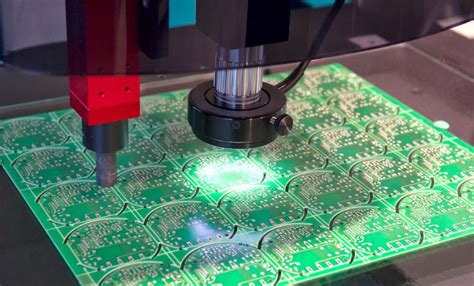
Visual inspection can be performed manually by trained operators or using automated optical inspection (AOI) equipment. AOI systems use high-resolution cameras and image processing software to quickly and accurately detect defects and measure critical dimensions on the board.
Electrical Testing
Electrical testing involves verifying the electrical performance and functionality of the PCB. This can include tests for continuity, insulation resistance, and impedance, as well as functional tests to ensure that the board operates as intended.
Electrical testing can be performed using specialized equipment, such as flying probe testers, boundary scan systems, or functional test fixtures. These tools can quickly and accurately identify electrical defects or performance issues that may not be visible through visual inspection.
Mechanical Testing
Mechanical testing involves verifying the physical properties and durability of the PCB. This can include tests for flexibility, vibration resistance, and thermal cycling, as well as measurements of dimensions, flatness, and warpage.
Mechanical testing is particularly important for PCBs that will be used in harsh environments or subjected to physical stress during use. These tests can help ensure that the board will maintain its structural integrity and performance over its intended lifespan.
Statistical Process Control
Statistical process control (SPC) is a method for monitoring and controlling the manufacturing process to ensure consistent quality and minimize defects. SPC involves collecting data on critical process parameters, such as copper thickness, hole size, and alignment, and using statistical analysis to identify trends or anomalies that may indicate a problem.
SPC can help PCB manufacturers identify and correct issues before they result in defective products, reducing waste and improving yields. SPC data can also be used to optimize the manufacturing process over time, leading to continuous improvements in quality and efficiency.
Frequently Asked Questions (FAQ)
-
What are the most common PCB tolerances that designers need to consider?
The most common PCB tolerances include dimensional tolerances (e.g., board thickness, outline, and hole size), copper thickness tolerances, spacing tolerances (e.g., conductor width and spacing), alignment tolerances, and soldermask and silkscreen tolerances. -
How do PCB tolerances affect the cost and lead time of a project?
Tighter PCB tolerances generally increase the cost and lead time of a project, as they require more advanced manufacturing processes, equipment, and materials. Looser tolerances can reduce costs and improve yields but may not be suitable for all applications. -
What are the most widely used industry standards for PCB tolerances?
The most widely used industry standards for PCB tolerances are those developed by the IPC (Association Connecting Electronics Industries), including IPC-6012 for rigid PCBs, IPC-6013 for flexible PCBs, IPC-2221 for PCB design, and IPC-7351 for land pattern geometries. -
How can designers ensure that their PCBs can be manufactured reliably and cost-effectively?
Designers can ensure manufacturability and cost-effectiveness by considering the capabilities and limitations of the intended manufacturing process, using standard components and footprints, allowing for adequate clearances and spacing, specifying appropriate tolerances for critical features, and communicating clearly with the manufacturing partner. -
What are some common methods for testing and verifying PCB tolerances after manufacturing?
Common methods for testing and verifying PCB tolerances include visual inspection (manual or automated), electrical testing (e.g., continuity, insulation resistance, and functional tests), mechanical testing (e.g., flexibility, vibration, and thermal cycling), and statistical process control (SPC) to monitor and optimize the manufacturing process.
In conclusion, understanding and managing manufacturing tolerances is a critical aspect of PCB design and production. By considering the factors that affect tolerances, following industry standards and best practices, and working closely with manufacturing partners, designers can ensure that their PCBs are manufactured reliably, cost-effectively, and to the highest quality standards. Effective testing and verification methods can further ensure that the final product meets the required tolerances and performance specifications, minimizing the risk of defects, failures, or customer returns. As PCB technology continues to evolve and advance, staying up-to-date with the latest tolerance requirements and manufacturing capabilities will be essential for success in this dynamic and demanding industry.
No responses yet