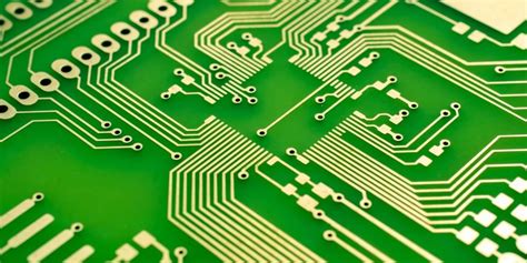
What is a PCB?
A printed circuit board, or PCB, is the foundation that supports and connects electronic components using conductive pathways, tracks or signal traces etched from laminated sheets of copper. It is the platform upon which nearly all modern electronic devices are built.
PCBs offer several advantages over other wiring methods:
- Compact size
- Reduced wiring errors
- Improved reliability
- Easier mass production
- Lower manufacturing costs
Types of PCBs
There are three main types of printed circuit boards:
| PCB Type | Layers | Application |
|---|---|---|
| Single-sided | One copper layer | Simple circuits |
| Double-sided | Two copper layers | Increased circuit density |
| Multi-layer | Three or more layers | Complex/high-speed circuits |
- Single-sided PCBs have components on one side and conductor pattern on the opposite side. They are easy to design and manufacture but have limited circuit density.
- Double-sided PCBs have components and conductors on both sides. Plated through-holes called vias allow connection between the layers. Double-sided boards support more complex circuitry.
- Multi-layer PCBs contain three or more conductive copper layers with insulating layers in between. The inner layers allow complex interconnections and reduce electromagnetic interference (EMI). High-speed digital and RF circuits use multi-layer construction.
How are PCBs Made?
The PCB manufacturing process turns a schematic circuit design into a finished physical board. While the exact steps can vary, the general process flow is:
- Design – Engineer captures the schematic and lays out the PCB
- Fabrication – Raw PCB is manufactured
- Assembly – Components are soldered to the board
- Testing – Assembled PCB is tested for proper functionality
Let’s examine each of these steps in more detail.
PCB Design
Every PCB starts as a circuit schematic – a diagram that shows how the electronic components connect together electrically. The schematic is then turned into a physical PCB layout that determines component placement and traces.
PCB design software is used to perform schematic capture and PCB layout. Popular PCB design tools include:
- Autodesk Eagle
- Altium Designer
- KiCad
- OrCAD
The PCB layout must follow design rules to ensure the board is manufacturable, meets specifications, and functions properly. Key considerations include:
- Selecting the optimal layer stack-up
- Component placement to minimize trace length
- Trace width and spacing to handle current loads
- Minimizing crosstalk and EMI
- Designing proper power distribution
- Performing signal integrity analysis
PCB Fabrication
Once the PCB layout is complete, fabrication files called Gerber files are generated and sent to a PCB manufacturer. The fabrication process typically follows these steps:
- Print photoresist film of circuit pattern on copper clad laminate
- Chemically etch exposed copper to remove unwanted copper
- Drill holes for component leads and vias
- Plate through-holes to connect top and bottom layers
- Apply solder mask over bare copper
- Silkscreen component legends
- Apply surface finish to prevent oxidation
Different laminate materials are available to meet application requirements for thermal performance, mechanical strength, and dielectric properties. The most common material is FR-4, a glass-reinforced epoxy laminate.
PCB Assembly
After the raw PCB is fabricated, electronic components need to be soldered to the board. The primary PCB assembly methods are:
- Through-hole technology (THT) – Component leads are inserted through drilled holes and soldered on the opposite side. THT components are hand soldered or wave soldered.
- Surface-mount technology (SMT) – Components are soldered directly to pads on the PCB surface. SMT allows for smaller components and denser circuit boards. Components are positioned via pick-and-place machines and soldered using reflow ovens.
SMT is the most common assembly method due to its efficiency and ability to handle high component density. However, some applications still use through-hole components when needed for high power devices, mechanical strength or connector interfaces.
PCB Testing
Before a PCB is put into use, it must be thoroughly tested to ensure it performs as intended. Testing occurs at multiple stages:
- Bare board testing verifies proper continuity between pins and isolation between networks. Automated optical inspection (AOI) also checks copper patterns and drills for defects.
- In-circuit testing (ICT) verifies component placement and solder joints after assembly. Flying probe and bed-of-nails testers make contact with test points on the board.
- Functional circuit testing (FCT) powers on the board and runs it through operational tests to validate performance.
Boundary scan testing using JTAG provides an integrated method to test connectivity and find faults on the board.
Any problems found during testing are debugged and corrected. The board may need to be reworked or go through additional design revisions before being approved for production.
PCB Design Considerations
Achieving a successful PCB design requires careful planning and attention to detail. This section covers major electrical, mechanical and manufacturing considerations to keep in mind.
Schematic Design
The first step in PCB design is schematic capture. Best practices for drawing schematics include:
- Use standard symbols for components
- Label all pins with names and numbers
- Provide values for all components
- Include voltage/current ratings where applicable
- Add notes to explain non-obvious functionality
Component Selection
Selecting the right components is critical for circuit performance, reliability and manufacturability. Consider these factors:
- Electrical ratings – Voltage, current, power, frequency
- Operating temperature range
- Package type – Through-hole or surface-mount
- Footprint and pin compatibility
- Availability and cost
Use trusted component vendors and authorized distributors to avoid counterfeit parts.
Layer Stack-up
The number of layers and their arrangement in the PCB stack-up dictates the routing density and impedance control. Work with your manufacturer to select the best stack-up for signal integrity and EMI performance.
Some general guidelines:
- Use even number of layers if possible
- Dedicate layers for power and ground planes
- Provide adequate spacing between signal layers
- Follow controlled impedance rules for high-speed signals
Power Distribution
Proper power distribution is essential to provide clean, stable voltage and current to all devices. Key considerations are:
- Use appropriate plane shapes and sizes
- Define power regions to isolate noisy circuits
- Place decoupling capacitors close to ICs
- Size traces to handle maximum current
- Perform IR drop analysis
Signal Integrity
Maintaining good signal integrity is critical for high-speed PCBs to function reliably. Some best practices are:
- Route critical signals on inner layers between planes
- Avoid crossing split planes with signals
- Match trace lengths to prevent timing skew
- Terminate transmission lines properly
- Perform simulation to verify signal integrity
Grounding
A low-impedance ground is essential for signal quality and EMI reduction. Ground plane best practices include:
- Flood all unused areas with copper
- Use ground pour on both sides for double-sided boards
- Stitch around plane edges and route gaps
- Provide multiple paths for return current
Thermal Management
Maintaining PCB temperatures within acceptable limits is important for reliability. Heat generated by components must be distributed and removed. Some thermal management techniques are:
- Use large plane areas for heat spreading
- Provide thermal vias and pads under hot components
- Increase copper weights of planes and traces
- Maximize airflow over the board
- Use heatsinks and fans in extreme cases
Manufacturing Considerations
Designing a PCB that is easy to manufacture is important for reducing production time and cost. Follow these guidelines:
- Adhere to minimum trace and space widths
- Provide adequate annular rings for vias
- Avoid acute angles in trace routing
- Follow solder mask and silkscreen clearances
- Consider panelization for efficient assembly
Work closely with your PCB fabrication and assembly partners to understand their capabilities and design rules.

PCB File Formats
Different file formats are used to exchange PCB design data between tools and manufacturers. The main formats to be familiar with are:
- Gerber – Vector image format for each PCB layer. Includes copper layers, solder mask, silk screen and drill data.
- ODB++ – Unified database format that includes all PCB layer data and netlists in one file. Intelligent format that avoids inconsistencies possible with Gerber.
- IPC-2581 – Emerging open standard that is intended to replace Gerber. An intelligent format that includes stackup, netlist and material information.
- STEP – 3D CAD format used for mechanical integration. Important for enclosure design and checking component clearances.
- BOM – Bill of materials that lists all components used on the PCB. Typically a spreadsheet file used for procurement and assembly.
Be sure to use the current file format versions and check your output with a free Gerber viewer before sending out for manufacturing.

Frequently Asked Questions
What are the steps involved in the PCB design process?
The key steps in designing a PCB are:
- Schematic capture
- Component selection and sourcing
- PCB layout and routing
- Design rule checks (DRC)
- Generate manufacturing files
- Prototyping and testing
- Design revisions
- Production
What software is used for PCB design?
Popular PCB design software includes:
- Autodesk Eagle
- Altium Designer
- Cadence OrCAD/Allegro
- Mentor Graphics PADS
- KiCad (free/open-source)
The choice of tools depends on the complexity of the design, team collaboration needs, and budget.
How long does it take to design a PCB?
PCB design time depends on the size and complexity of the board. A simple single-sided PCB can be designed in a few hours, while a large multi-layer board with high-speed interfaces and analog/RF circuits can take several weeks.
On average, allow the following design times:
| Board Complexity | Design Time |
|---|---|
| Simple (< 50 components) | 1-2 days |
| Moderate (50-200 components) | 1-2 weeks |
| Complex (> 200 components) | 4-8 weeks |
Remember to budget additional time for design revisions and prototyping. Working with an experienced PCB design firm can help you meet your time-to-market goals.
What are some common PCB Design Mistakes to avoid?
Avoid these common PCB design pitfalls:
- Incorrect schematic (e.g. missing connections, wrong pinouts)
- Violating component ratings (e.g. overvoltage, overcurrent)
- Insufficient decoupling on power pins
- Inadequate spacing between traces and components
- Forgetting to include test points
- Not following controlled impedance rules
- Improper termination of high-speed signals
- Insufficient thermal management
- Not adhering to manufacturing constraints
Careful planning, adherence to best design practices, and thorough design reviews can prevent these costly mistakes.
How much does it cost to manufacture a PCB?
PCB fabrication and assembly costs depend on the number of layers, size, materials, surface finish, and quantity. Typical prices for a 2-layer board are:
| Quantity | Prototype | Mid Volume | High Volume |
|---|---|---|---|
| 1-5 | $50-$500 ea | – | – |
| 100 | $5-$15 ea | $3-$10 ea | – |
| 1000 | – | $2-$5 ea | $1-$3 ea |
| 10000 | – | – | < $1 ea |
Note that these prices are rough estimates – your actual costs will depend on your specific PCB requirements. Get quotes from multiple PCB shops to compare pricing and lead times.
Conclusion
Congratulations, you now have a solid foundation in PCB design principles! By understanding the PCB manufacturing process, design considerations and file formats, you’ll be able to confidently design boards that are manufacturable, reliable and meet performance goals.
Remember, PCB design is a complex field that takes years to master. Don’t be afraid to consult with experienced engineers and PCB design firms for guidance on your projects. With practice and attention to detail, you’ll be designing successful PCBs in no time.
No responses yet