What are PCBs?
PCBs are flat boards made of insulating materials, such as fiberglass or plastic, with conductive pathways etched or printed onto their surface. These pathways, also known as traces, connect various electronic components, such as resistors, capacitors, and integrated circuits (ICs), to form a complete electronic circuit.
Types of PCBs
There are several types of PCBs, each designed to meet specific requirements and applications:
-
Single-Sided PCBs: These boards have conductive traces on only one side of the insulating substrate. They are the simplest and most cost-effective type of PCB, suitable for low-complexity circuits.
-
Double-sided PCBs: These boards have conductive traces on both sides of the insulating substrate, allowing for more complex circuit designs and higher component density. The two sides are connected using through-hole technology or vias.
-
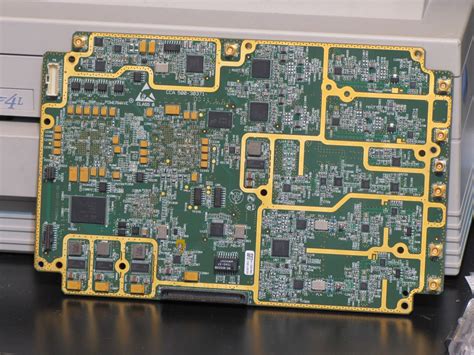
Multi-layer PCBs: These boards consist of multiple layers of insulating material and conductive traces stacked together. They offer the highest level of complexity and component density, making them suitable for advanced electronic devices.
-
Flexible PCBs: These boards are made of flexible insulating materials, such as polyimide, allowing them to bend and conform to various shapes. They are commonly used in wearable devices, medical equipment, and aerospace applications.
-
Rigid-flex PCBs: These boards combine the benefits of rigid and flexible PCBs, featuring both rigid and flexible sections. They offer the reliability of rigid boards and the flexibility needed for compact or movable designs.
The Manufacturing Process of PCBs
The manufacturing process of PCBs involves several steps, each requiring precision and expertise to ensure the quality and reliability of the final product.
Design and Prototyping
-
Schematic design: The first step in creating a PCB is to develop a schematic diagram that represents the electronic circuit. This diagram shows the components and their connections, serving as a blueprint for the PCB layout.
-
PCB layout: Using specialized software, PCB designers create a physical layout of the circuit based on the schematic diagram. The layout determines the placement of components, the routing of traces, and the overall size and shape of the PCB.
-
Prototyping: Before mass production, a prototype of the PCB is created to test its functionality and identify any potential issues. Prototypes can be made using various methods, such as 3D printing or CNC milling.
Fabrication
-
Substrate preparation: The insulating substrate, typically made of fiberglass or plastic, is cut to the desired size and shape.
-
Copper lamination: A thin layer of copper is laminated onto the substrate using heat and pressure. For double-sided or multi-layer PCBs, this process is repeated for each layer.
-
Drilling: Holes are drilled into the substrate to accommodate through-hole components and create vias for connecting different layers in multi-layer PCBs.
-
Patterning: The copper layer is patterned using a photolithography process. A photoresist layer is applied to the copper, and the desired circuit pattern is transferred using UV light exposure and chemical etching.
-
Plating: The exposed copper traces and holes are plated with a thin layer of another metal, such as tin, nickel, or gold, to protect the copper from oxidation and improve solderability.
-
Solder mask application: A protective layer called solder mask is applied to the PCB, covering the areas where soldering is not required. This layer also provides insulation and protection against short circuits.
-
Silkscreen printing: Text, logos, and component identifiers are printed onto the PCB using a silkscreen process, making it easier to assemble and troubleshoot the board.
Assembly
-
Component placement: Electronic components are placed on the PCB, either manually or using automated pick-and-place machines. Surface-mount devices (SMDs) are placed directly onto the pads, while through-hole components are inserted into the drilled holes.
-
Soldering: The PCB is heated, and solder is applied to the component leads and pads, creating a strong electrical and mechanical connection. This can be done using wave soldering, reflow soldering, or hand soldering techniques.
-
Inspection and testing: The assembled PCB undergoes visual inspection and various electrical tests to ensure proper functionality and identify any defects or shorts.

Applications of PCBs
PCBs are used in a wide range of industries and applications, showcasing their versatility and importance in modern technology.
Consumer Electronics
PCBs are the foundation of most consumer electronic devices, such as:
- Smartphones and tablets
- Laptops and desktop computers
- Televisions and displays
- Gaming consoles and controllers
- Smart home devices
Industrial Automation and Control Systems
PCBs play a crucial role in industrial automation and control systems, enabling the monitoring and regulation of various processes. Examples include:
- Programmable Logic Controllers (PLCs)
- Human-Machine Interfaces (HMIs)
- Sensors and actuators
- Motor drives and power electronics
Medical Devices
PCBs are essential components in medical devices, ensuring reliability, accuracy, and safety. Some examples include:
- Patient monitoring systems
- Diagnostic imaging equipment
- Implantable devices (e.g., pacemakers, cochlear implants)
- Surgical instruments and robots
Automotive Electronics
Modern vehicles heavily rely on PCBs for various electronic systems, such as:
- Engine control units (ECUs)
- Infotainment systems
- Advanced driver assistance systems (ADAS)
- Electric vehicle battery management systems
Aerospace and Defense
PCBs designed for aerospace and defense applications must meet stringent requirements for reliability, durability, and performance under extreme conditions. Examples include:
- Avionics systems
- Satellite communications
- Radar and surveillance equipment
- Missile guidance systems

The Importance of PCB Design and Manufacturing Quality
The quality of PCB design and manufacturing directly impacts the performance, reliability, and longevity of electronic devices. Poor design or manufacturing can lead to various issues, such as:
- Signal integrity problems
- Electromagnetic interference (EMI)
- Thermal management issues
- Premature component failure
- Reduced product lifespan
To ensure the highest quality, PCB designers and manufacturers must adhere to industry standards, such as IPC (Association Connecting Electronics Industries) standards. These standards provide guidelines for design, fabrication, assembly, and testing of PCBs, ensuring consistency and reliability across the industry.

Future Trends in PCB Technology
As electronic devices continue to advance and new technologies emerge, PCB design and manufacturing must also evolve to keep pace. Some of the future trends in PCB technology include:
Miniaturization
The demand for smaller, more compact electronic devices is driving the need for miniaturized PCBs. This trend involves the use of smaller components, higher component density, and advanced packaging techniques, such as system-in-package (SiP) and 3D packaging.
High-Speed and High-Frequency PCBs
With the increasing demand for faster data transmission and higher bandwidth, PCBs designed for high-speed and high-frequency applications are becoming more prevalent. These PCBs require specialized design techniques, materials, and manufacturing processes to minimize signal integrity issues and ensure reliable performance.
Environmentally-Friendly Materials and Processes
As environmental concerns grow, the PCB industry is shifting towards more sustainable and eco-friendly materials and processes. This includes the use of halogen-free and lead-free materials, as well as the adoption of green manufacturing practices that reduce waste and energy consumption.
Intelligent and Connected PCBs
The rise of the Internet of Things (IoT) and Industry 4.0 is driving the development of intelligent and connected PCBs. These boards incorporate sensors, communication modules, and processing capabilities, enabling them to collect, process, and transmit data in real-time.
Frequently Asked Questions (FAQ)
- What are the advantages of using PCBs over point-to-point wiring?
PCBs offer several advantages over point-to-point wiring, including: - Improved reliability and consistency
- Reduced wiring errors and short circuits
- Easier troubleshooting and maintenance
- Increased automation in manufacturing
-
Compact and space-saving designs
-
How do I choose the right type of PCB for my application?
When selecting the right type of PCB for your application, consider factors such as: - Circuit complexity and component density
- Required electrical performance and signal integrity
- Mechanical requirements (size, shape, and flexibility)
- Environmental conditions (temperature, humidity, and vibration)
-
Budget and production volume
-
What is the difference between through-hole and surface-mount technology (SMT)?
Through-hole technology involves components with leads that are inserted into holes drilled in the PCB and soldered on the opposite side. SMT, on the other hand, involves components that are placed directly onto the surface of the PCB and soldered using reflow or wave soldering techniques. SMT allows for smaller components and higher component density, while through-hole technology is more robust and easier to replace components. -
How can I ensure the quality and reliability of my PCBs?
To ensure the quality and reliability of your PCBs: - Follow industry standards and best practices for design and manufacturing
- Use high-quality materials and components from reputable suppliers
- Implement rigorous testing and inspection procedures throughout the manufacturing process
- Work with experienced and certified PCB manufacturers
-
Conduct regular quality audits and continuously improve processes
-
What are the challenges in designing and manufacturing high-speed PCBs?
Designing and manufacturing high-speed PCBs present several challenges, including: - Managing signal integrity issues, such as crosstalk, reflections, and impedance mismatch
- Minimizing electromagnetic interference (EMI) and ensuring electromagnetic compatibility (EMC)
- Selecting appropriate materials with suitable dielectric properties
- Implementing advanced layout techniques, such as controlled impedance routing and differential pair routing
- Ensuring precise manufacturing processes to maintain tight tolerances and minimize variations
Conclusion
PCBs are the unsung heroes of the electronic world, enabling the development and advancement of countless technologies that shape our modern society. From consumer electronics to medical devices, automotive systems to aerospace applications, PCBs play a vital role in ensuring the functionality, reliability, and performance of these devices.
As technology continues to evolve, so too must the design and manufacturing of PCBs. By staying at the forefront of industry trends, adopting best practices, and continuously improving processes, PCB designers and manufacturers can meet the ever-growing demands of the electronic industry and contribute to the development of innovative solutions that address the challenges of the future.
Tables
Comparison of Different PCB Types
| PCB Type | Layers | Complexity | Cost | Applications |
|---|---|---|---|---|
| Single-sided | 1 | Low | Low | Simple circuits, low-power devices |
| Double-sided | 2 | Medium | Medium | Moderate complexity circuits, power supplies |
| Multi-layer | 3+ | High | High | Complex circuits, high-speed devices, smartphones |
| Flexible | 1-2 | Low to Medium | Medium to High | Wearables, medical devices, aerospace |
| Rigid-Flex | 2+ | High | High | Compact devices, movable parts, high-reliability applications |
PCB Manufacturing Process Overview
| Step | Process | Description |
|---|---|---|
| 1 | Design and Prototyping | Schematic design, PCB layout, and prototyping |
| 2 | Substrate Preparation | Cutting and cleaning of the insulating substrate |
| 3 | Copper Lamination | Laminating a thin layer of copper onto the substrate |
| 4 | Drilling | Drilling holes for through-hole components and vias |
| 5 | Patterning | Transferring the circuit pattern onto the copper layer |
| 6 | Plating | Plating exposed copper traces and holes with a protective metal |
| 7 | Solder Mask Application | Applying a protective layer to insulate and protect the PCB |
| 8 | Silkscreen Printing | Printing text, logos, and component identifiers onto the PCB |
| 9 | Component Placement | Placing electronic components onto the PCB |
| 10 | Soldering | Soldering components to create electrical and mechanical connections |
| 11 | Inspection and Testing | Visual inspection and electrical testing to ensure functionality |
By understanding the importance of PCBs, their manufacturing process, and their applications in various industries, we can better appreciate the critical role they play in our technology-driven world. As we continue to push the boundaries of innovation, PCBs will undoubtedly remain at the heart of electronic devices, enabling us to create smarter, faster, and more efficient solutions for the challenges of tomorrow.
No responses yet