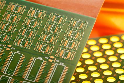
Understand the PCB Manufacturing Process
Before diving into specific design guidelines, it’s important to have a basic understanding of how PCBs are manufactured. The typical steps in PCB fabrication are:
- Material selection and preparation
- Imaging and etching copper layers
- Lamination of layers
- Drilling holes
- Plating holes and exposed copper
- Applying solder mask and silkscreen
- Surface finish (e.g. HASL, ENIG, OSP)
- Electrical testing and inspection
Having awareness of this process will help inform design decisions to ensure your board can be reliably and cost-effectively produced.
Choose the Right Number of Layers
One of the first decisions in any PCB design is selecting the appropriate number of copper layers. This depends on the complexity of the circuitry, component density, signal integrity requirements, power delivery needs, and cost constraints.
Here are some general guidelines for choosing the number of layers:
| Complexity | Typical Layer Count |
|---|---|
| Simple, low-density analog/digital | 1-2 |
| Moderate complexity, medium density | 4 |
| Complex, high speed, dense BGAs | 6-8 |
| Very complex, DDR3/4, high layer count FPGAs | 10+ |
Keep in mind that higher layer counts increase cost and manufacturing time. Be judicious and try to minimize layer count where possible. Work with your fabrication partner to understand their capabilities and tradeoffs between different layer counts and materials.

Follow Good High Speed Design Practices
With rising clock frequencies and edge rates, signal integrity is more critical than ever. Poor high speed design practices can lead to EMI issues, signal degradation, and even complete device malfunction.
Some important high speed PCB Design Guidelines include:
- Route critical signals first, on inner layers between power/ground planes when possible
- Maintain consistent impedance for controlled impedance traces (e.g. clock, memory, RF lines)
- Keep high speed traces as short and direct as possible
- Avoid using stubs or unterminated traces
- Provide solid power and ground planes and decouple ICs properly
- Use sufficient ground vias and stitching
- Space high speed signal traces apart to minimize crosstalk
- Simulate and measure signal integrity during design

Optimize Power Delivery
Proper power delivery network (PDN) design is essential for providing clean, stable power to ICs and minimizing EMI. Key considerations include:
- Use appropriate plane layer stacks (e.g. multi-layer boards should have power and ground planes)
- Determine appropriate copper weights for planes based on current demands
- Place decoupling capacitors close to IC power pins
- Use correct via sizes and quantities for stitching planes together
- Simulate and measure PDN impedance to validate design
Here are some typical decoupling capacitor arrangements:
| Configuration | Description |
|---|---|
| Bulk decoupling | Large value (e.g. 10 μF) capacitors near Voltage Regulators to stabilize voltage |
| Local decoupling | Small/medium value (e.g. 0.1 μF) caps very close to IC power pins for high freq. transients |
| Distributed decoupling | Medium value caps spread evenly across PCB to lower overall PDN impedance |
The goal is to minimize PDN impedance across the required frequency range. Impedance should be kept below a target level, commonly 0.1 ohm for digital ICs.

Consider DFM and DFA
Design for manufacturability (DFM) and design for assembly (DFA) are critical for ensuring your PCB can be reliably and cost-effectively fabricated and assembled. Involve your manufacturing partners early in the design process and adhere to their DFM/DFA guidelines.
Some important DFM considerations:
- Adhere to manufacturer’s capabilities and tolerances for trace/space, hole sizes, Annular rings, etc.
- Avoid acid traps and provide sufficient etch-compensated traces
- Provide teardrops on traces entering pads and vias
- Follow solder mask and silkscreen clearance rules
- Panelize boards properly for fabrication
Key DFA guidelines include:
- Place components on a grid to allow efficient automated assembly
- Orientate components in the same direction where possible
- Avoid overhanging or physically interfering components
- Comply with component pitch and spacing requirements for assembly
- Provide clear silkscreen component polarity and designator markings
- Ensure test point and probe access for testing
Create a Robust Mechanical Design
The mechanical aspects of a PCB, such as material selection, dimensions, mounting, and heatsinking are just as important as the electrical design.
Some mechanical design best practices:
- Choose appropriate PCB material and copper weights for your application (e.g. FR-4, PTFE, metal core)
- Define proper board thickness and dimensions with mounting holes for enclosure
- Adhere to component height restrictions and create 3D models to verify mechanical clearances
- Consider thermal requirements and provide thermal reliefs, heatsinks, and vias under hot components
- Minimize board flex and strain on components in systems undergoing mechanical stress
Document and Communicate Your Design
Thorough documentation and clear communication are essential for successfully bringing a PCB from design through manufacturing. Key files to produce include:
- Schematic with clear hierarchical structure and naming
- Bill of Materials (BOM) with manufacturer part numbers, quantities, and alternates
- Layout files in standard CAD formats (e.g. ODB++, Gerber, IPC-2581)
- Assembly drawings clearly showing component placements and orientations
- Fabrication drawings with stackups, drill data, detailed dimensions and tolerances
- 3D STEP models for mechanical integration
Collaborate closely with your entire design team as well as your manufacturing partners. Implement a design review process to catch errors early and ensure all stakeholders are on the same page.
Frequently Asked Questions
What are some common PCB Design Mistakes to avoid?
Some of the most common PCB design mistakes include:
- Violating spacing and clearance rules leading to shorts or manufacturing issues
- Incorrect hole and via sizes for manufacturing capabilities
- Lack of proper grounding, shielding, or power decoupling
- Poor high speed routing topologies introducing signal integrity problems
- Insufficient cooling for thermal demands
- Inadequate documentation for manufacturing
How do I select the right PCB material for my design?
The choice of PCB material depends on several factors such as:
- Electrical performance (dielectric constant, dissipation factor)
- Thermal requirements (glass transition temp, thermal conductivity)
- Mechanical needs (flexibility, strength, water absorption)
- Frequency of operation (loss tangent at operating frequencies)
- Cost and availability
The most common material for general purpose use is FR-4. For high freq or thermal applications, materials like Rogers, Isola, or PTFE may be preferable. Consult with your fabrication shop on available materials for your needs and budget.
What tools are used for PCB design and layout?
There are many PCB design tools on the market, ranging from simple to full-featured. Some of the most popular include:
- Altium Designer
- Cadence Allegro/OrCAD
- Autodesk EAGLE
- KiCad (open source)
- Mentor Graphics PADS
Modern PCB design software will include schematic capture, library management, 2D layout, and 3D modeling capabilities. More advanced tools may have signal/power integrity simulation, Rigid-Flex Design, and PLM integration. Choose the tool that fits your design needs and budget.
How do I ensure my PCB will be manufacturable?
To ensure your PCB is manufacturable, follow these steps:
-
Engage with your fabrication and assembly partners early in the design process to understand their capabilities and design rules.
-
Use a PCB design tool that enables definition of design rules and constraints. Perform DRCs continuously while laying out the board.
-
Follow industry standards for footprints, pad sizes, drill holes, clearances, etc. such as the IPC-7351B land pattern standard.
-
Create full documentation packages for fabrication and assembly, including Gerbers, drill files, BOMs, drawings, and pick and place files.
-
Communicate clearly with your manufacturers and promptly address any discrepancies or concerns. Implement a sign-off and design review process.
What are some future trends in PCB design?
Some notable trends in PCB design include:
- HDI (High Density Interconnect) technology becoming more common with finer trace/space and microvias
- Rigid-flex and multi-board modules enabling dense 3D packaging
- High speed signaling standards like PCIe 5.0, USB4, DDR5 memory pushing signaling bandwidths
- Tighter integration between electrical and mechanical CAD tools
- Increased automation of design rule checks, assembly, and testing
- Growing environmental regulations impacting material selection (e.g. REACH, RoHS)
Keeping pace with technology and adapting to new tools and standards is critical for PCB designers. Continuous learning and collaborating with industry groups and manufacturers is necessary.
Conclusion
Designing reliable, high-performance PCBs requires attention to detail and adherence to many guidelines and best practices. From choosing the layer count and managing high speed signals to optimizing manufacturability and thoroughly documenting your design, there are countless decisions to be made.
By understanding the manufacturing process, using appropriate design tools, collaborating with your manufacturers, and following industry standards and guides lines, you’ll be well on your way to creating successful PCBs. At the end of the day, a thoughtful, well-executed design is key to achieving reliable, cost-effective electronics that meet your application’s needs.
No responses yet