Introduction to PCB Panelization
PCB panelization is the process of arranging multiple printed circuit board (PCB) designs onto a single panel for manufacturing. This technique is widely used in the electronics industry to optimize production efficiency and reduce costs. By grouping several PCBs together, manufacturers can minimize material waste, streamline the assembly process, and improve overall productivity.
What is PCB Panelization?
PCB panelization involves combining multiple identical or different PCB designs onto a single large panel. The individual PCBs are arranged in a grid pattern, with spaces between each board to allow for separation after manufacturing. The panel is then processed as a single unit through the various stages of PCB fabrication, including drilling, plating, and solder mask application.
Benefits of PCB Panelization
-
Cost Reduction: By producing multiple PCBs on a single panel, manufacturers can reduce material waste and minimize the time and labor required for handling individual boards. This leads to lower production costs, which can be passed on to customers.
-
Increased Efficiency: Panelization streamlines the manufacturing process by allowing multiple PCBs to be processed simultaneously. This reduces the number of setups and changeovers required, resulting in faster production times and improved efficiency.
-
Consistent Quality: When PCBs are panelized, they undergo the same manufacturing processes together, ensuring consistent quality across all boards in the panel. This is particularly important for high-volume production runs where maintaining uniform quality is critical.
-
Simplified Assembly: Panelized PCBs are easier to handle and assemble compared to individual boards. The panels can be loaded onto pick-and-place machines or other automated assembly equipment, reducing the time and effort required for manual handling.
PCB Panelization Software
To efficiently design and prepare PCBs for panelization, specialized software tools are used. These tools provide a range of features and capabilities to streamline the panelization process and ensure optimal results.
Popular PCB Panelization Software
-
CAM350: Developed by DownStream Technologies, CAM350 is a comprehensive PCB panelization and CAM (Computer-Aided Manufacturing) software. It offers advanced features for panel layout, automatic and manual placement of PCBs, and generation of manufacturing files.
-
Pulsonix: Pulsonix is an integrated PCB design and panelization software that provides a user-friendly interface for creating panel layouts. It supports automatic and manual placement, copper balancing, and generation of manufacturing outputs.
-
Ucamco Integr8tor: Integr8tor is a powerful PCB panelization software that focuses on automation and optimization. It offers features like automatic panel creation, design rule checking (DRC), and intelligent Fiducial placement.
-
Zuken Panel Advisor: Panel Advisor is a panelization tool that integrates with Zuken’s PCB design software. It provides a streamlined workflow for panel creation, optimization, and manufacturing data generation.
Key Features of PCB Panelization Software
-
Automatic and Manual Placement: PCB panelization software allows users to automatically arrange PCBs on a panel based on predefined rules and constraints. Manual placement options are also available for fine-tuning the layout.
-
Design Rule Checking (DRC): DRC features ensure that the panelized design meets manufacturing requirements and constraints. This includes checking for minimum spacing, copper balancing, and other design rules specific to the fabrication process.
-
Manufacturing Output Generation: Panelization software generates the necessary manufacturing files, such as Gerber files, drill files, and pick-and-place data, for the panelized design. These files are used by the fabrication and assembly facilities to produce the PCBs.
-
Customizable Templates and Libraries: Many panelization tools provide customizable templates and libraries for common panel sizes, tooling holes, and Fiducial Markers. This allows users to quickly set up panels based on their specific manufacturing requirements.

PCB Panelization Techniques
There are various techniques used in PCB panelization to ensure the efficient and reliable separation of individual boards from the panel. The choice of technique depends on factors such as the PCB design, material, and manufacturing constraints.
Tab Routing
Tab routing involves creating small tabs or bridges between the individual PCBs on the panel. These tabs hold the boards in place during manufacturing and are later removed to separate the PCBs. The tabs are typically designed to be easily breakable, allowing for manual separation without damaging the boards.
Advantages:
– Simple and cost-effective method
– Suitable for low-volume production
– Allows for easy manual separation of boards
Disadvantages:
– Manual separation can be time-consuming for high-volume production
– Risk of damage to the PCBs during separation
– Limited control over the break-out process
V-Scoring
V-scoring is a technique where V-shaped grooves are cut into the panel along the edges of the individual PCBs. The grooves are cut partially through the panel, leaving a thin layer of material that holds the boards together. After manufacturing, the PCBs can be easily snapped out of the panel along the V-scored lines.
Advantages:
– Provides a clean and controlled break-out process
– Reduces the risk of damage to the PCBs during separation
– Suitable for high-volume production
Disadvantages:
– Requires specialized equipment for V-scoring
– May not be suitable for thick or rigid PCB materials
– Can add additional cost to the manufacturing process
Perforated Tabs
Perforated tabs are a combination of tab routing and V-scoring techniques. Small perforations or holes are drilled along the edges of the individual PCBs, creating a perforated line. The PCBs can then be easily separated from the panel by breaking along the perforated lines.
Advantages:
– Provides a controlled and predictable break-out process
– Reduces the risk of damage to the PCBs during separation
– Suitable for a wide range of PCB materials and thicknesses
Disadvantages:
– Requires additional drilling or punching operations
– May add cost and complexity to the manufacturing process
– Perforations can affect the edge quality of the separated PCBs
Comparison of Panelization Techniques
| Technique | Ease of Separation | Control over Break-out | Suitability for High-Volume | Cost |
|---|---|---|---|---|
| Tab Routing | Easy | Limited | Low | Low |
| V-Scoring | Moderate | Good | High | Moderate |
| Perforated Tabs | Easy | Good | High | Moderate to High |

Best Practices for PCB Panelization
To ensure successful PCB panelization and manufacturing, consider the following best practices:
-
Consult with the PCB Manufacturer: Engage with your PCB manufacturer early in the design process to discuss their specific panelization requirements and guidelines. They can provide valuable insights and recommendations based on their manufacturing capabilities and experience.
-
Consider Panel Size and Utilization: Optimize the panel size and utilization to minimize material waste and maximize production efficiency. Work with your manufacturer to determine the optimal panel dimensions and layout for your specific PCB design.
-
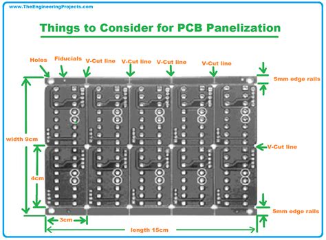
Maintain Proper Spacing and Clearances: Ensure adequate spacing between individual PCBs on the panel to allow for safe separation and to avoid interference during manufacturing. Follow the manufacturer’s guidelines for minimum spacing and clearances.
-
Use Standardized Fiducial Markers: Include standardized fiducial markers on the panel to facilitate accurate alignment and registration during the manufacturing process. Consult with your manufacturer for their preferred fiducial marker specifications.
-
Balance Copper Distribution: Ensure an even distribution of copper across the panel to minimize warpage and maintain flatness during manufacturing. Use copper balancing techniques, such as adding copper fills or dummy components, to achieve a balanced copper distribution.
-
Perform Design Rule Checks (DRC): Utilize the DRC features in your panelization software to verify that the panelized design meets all manufacturing constraints and requirements. This includes checking for minimum spacing, copper balancing, and other design rules specific to the fabrication process.
-
Generate Accurate Manufacturing Files: Ensure that the generated manufacturing files, such as Gerber files and drill files, accurately represent the panelized design. Double-check the files for completeness and correctness before submitting them to the manufacturer.
-
Communicate and Collaborate: Maintain open communication and collaboration with your PCB manufacturer throughout the panelization and manufacturing process. Clearly convey your requirements, expectations, and any special considerations to ensure a smooth and successful production run.

Frequently Asked Questions (FAQ)
- What is the purpose of PCB panelization?
-
PCB panelization is used to arrange multiple PCB designs onto a single panel for efficient manufacturing. It helps reduce material waste, streamline the assembly process, and improve overall production efficiency.
-
Can different PCB designs be panelized together?
-
Yes, different PCB designs can be panelized together on a single panel, provided they have similar manufacturing requirements and constraints. However, it is more common to panelize identical or similar PCB designs to maintain consistency and simplify the manufacturing process.
-
How do I choose the right panelization technique for my PCB?
-
The choice of panelization technique depends on factors such as the PCB design, material, manufacturing constraints, and production volume. Consult with your PCB manufacturer to determine the most suitable technique for your specific requirements.
-
What are the common challenges in PCB panelization?
-
Common challenges in PCB panelization include ensuring proper spacing and clearances between boards, maintaining copper balance across the panel, and generating accurate manufacturing files. Careful planning, adherence to best practices, and collaboration with the PCB manufacturer can help mitigate these challenges.
-
How does PCB panelization impact the cost of manufacturing?
- PCB panelization can significantly reduce the cost of manufacturing by minimizing material waste, streamlining the assembly process, and improving production efficiency. By producing multiple PCBs on a single panel, manufacturers can optimize resource utilization and reduce the time and labor required for handling individual boards.
Conclusion
PCB panelization is a critical process in the manufacturing of printed circuit boards, enabling efficient and cost-effective production. By arranging multiple PCBs onto a single panel, manufacturers can optimize material usage, streamline the assembly process, and maintain consistent quality across the boards.
Specialized PCB panelization software tools provide the necessary features and capabilities to design and prepare panels for manufacturing. These tools offer automatic and manual placement options, design rule checking, and generation of manufacturing files.
Various panelization techniques, such as tab routing, V-scoring, and perforated tabs, are used to ensure the reliable separation of individual PCBs from the panel. The choice of technique depends on factors such as the PCB design, material, and manufacturing constraints.
To ensure successful PCB panelization, it is crucial to follow best practices, such as consulting with the PCB manufacturer, optimizing panel utilization, maintaining proper spacing and clearances, and performing design rule checks. Open communication and collaboration with the manufacturer throughout the process are essential for a smooth and successful production run.
By understanding the principles and techniques of PCB panelization, and leveraging the capabilities of panelization software, designers and manufacturers can efficiently produce high-quality PCBs while minimizing costs and maximizing productivity.
No responses yet