Introduction to PCB Prototyping
PCB prototyping is an essential step in the electronic product development process. It allows designers and engineers to test and validate their designs before committing to large-scale production. Small batch PCB assembly is particularly useful for creating prototypes and low-volume production runs, as it offers flexibility, speed, and cost-effectiveness compared to traditional high-volume manufacturing methods.
What is PCB Prototyping?
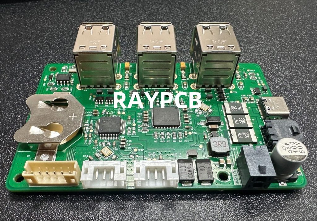
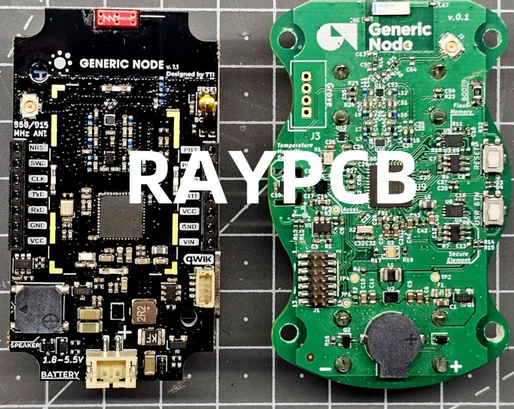
PCB prototyping is the process of creating a physical printed circuit board (PCB) based on a digital design. The purpose of prototyping is to test the functionality, performance, and reliability of the PCB design before mass production. Prototyping allows designers to identify and correct any issues or errors in the design, ensuring that the final product meets the desired specifications and requirements.
Benefits of Small Batch PCB Assembly
Small batch PCB assembly offers several advantages for prototyping and low-volume production:
- Flexibility: Small Batch assembly allows for quick design changes and iterations, enabling designers to refine their designs based on testing and feedback.
- Speed: Prototyping services often have shorter lead times compared to large-scale production, allowing for faster turnaround and time-to-market.
- Cost-effectiveness: Producing small quantities of PCBs is generally more cost-effective than committing to large production runs, especially for prototypes or low-volume products.
- Quality control: Small batch assembly allows for closer inspection and quality control of each PCB, ensuring that the prototypes meet the required standards.
PCB Prototyping Process
The PCB prototyping process typically involves several steps, from design to assembly and testing.
Step 1: PCB Design
The first step in PCB prototyping is to create a digital design of the circuit board using electronic design automation (EDA) software. The design includes the schematic diagram, component placement, and routing of the electrical connections. Designers must consider factors such as signal integrity, power distribution, and thermal management when creating the PCB layout.
Step 2: Design Review and Verification
Before proceeding with prototype fabrication, the PCB design undergoes a thorough review and verification process. This includes:
- Design rule check (DRC): Verifying that the design meets the manufacturing and assembly constraints, such as minimum trace width and spacing, hole sizes, and clearances.
- Electrical rule check (ERC): Checking for electrical issues, such as short circuits, open circuits, and incorrect connections.
- Signal integrity analysis: Simulating the signal behavior to ensure that the design meets the required performance and reliability standards.
Step 3: PCB Fabrication
Once the design is finalized and verified, the PCB Prototype is fabricated using a variety of methods, depending on the complexity and requirements of the design. Common fabrication techniques include:
- Subtractive process: Etching away unwanted copper from a pre-laminated board to create the desired circuit pattern.
- Additive process: Depositing conductive material onto a substrate to form the circuit pattern, such as inkjet printing or 3D printing.
- Milling: Using a computer-controlled milling machine to remove copper from a blank PCB, creating the circuit pattern.
Step 4: PCB Assembly
After the PCB is fabricated, the components are assembled onto the board. Small batch PCB assembly can be performed using various methods, such as:
- Hand assembly: Manually placing and soldering components onto the PCB, suitable for very low-volume prototypes or complex designs.
- Semiautomated assembly: Using a combination of automated equipment and manual labor to place and solder components, suitable for low to medium-volume production.
- Fully automated assembly: Employing automated pick-and-place machines and reflow ovens for component placement and soldering, suitable for higher-volume production and consistent quality.
Step 5: Testing and Validation
The assembled PCB prototype undergoes rigorous testing and validation to ensure that it functions as intended and meets the design specifications. This includes:
- Functional testing: Verifying that the PCB performs the desired functions and operates within the specified parameters.
- Environmental testing: Subjecting the PCB to various environmental conditions, such as temperature, humidity, and vibration, to assess its reliability and durability.
- Compliance testing: Ensuring that the PCB meets the relevant industry standards and regulations, such as electromagnetic compatibility (EMC) and safety requirements.

Choosing a PCB Prototyping Service
When selecting a PCB prototyping service for small batch assembly, consider the following factors:
Technical Capabilities
Ensure that the service provider has the necessary technical capabilities to handle your specific PCB design and assembly requirements. This includes:
- PCB fabrication technologies: Can they support the required PCB materials, layer counts, trace widths, and hole sizes?
- Component types: Do they have the capability to handle the specific components used in your design, such as surface mount devices (SMDs), ball grid arrays (BGAs), or through-hole components?
- Assembly methods: Can they offer the appropriate assembly methods for your prototype, such as hand assembly, semiautomated, or fully automated assembly?
Turnaround Time
One of the key advantages of small batch PCB assembly is the faster turnaround time compared to large-scale production. When choosing a prototyping service, consider their lead times for fabrication and assembly, and ensure that they can meet your project deadlines.
Quality Control
Quality control is critical in PCB prototyping to ensure that the assembled boards meet the design specifications and perform reliably. Look for a service provider that has a robust quality control process, including:
- Automated optical inspection (AOI): Using machine vision systems to detect assembly defects, such as missing or misaligned components.
- X-ray inspection: Employing X-ray imaging to inspect hidden solder joints, such as those under BGAs or chip-scale packages.
- Electrical testing: Performing functional and in-circuit tests to verify the electrical performance of the assembled PCBs.
Cost and Minimum Order Quantity (MOQ)
Small batch PCB assembly services often have higher unit costs compared to large-scale production due to the lower volumes and higher setup costs. However, they typically offer lower minimum order quantities (MOQs), making them more accessible for prototyping and low-volume projects. When comparing service providers, consider their pricing structure and MOQs to ensure that they align with your project budget and requirements.

Best Practices for PCB Prototyping
To ensure successful PCB prototyping and small batch assembly, follow these best practices:
Design for Manufacturing (DFM)
Design your PCB with manufacturing and assembly considerations in mind. This includes:
- Adhering to the fabrication and assembly constraints, such as minimum trace widths, spacing, and hole sizes.
- Selecting components that are readily available and compatible with the chosen assembly methods.
- Providing clear and complete documentation, including bill of materials (BOM), assembly drawings, and fabrication files.
Collaboration and Communication
Maintain open and regular communication with your PCB prototyping service provider throughout the project. This includes:
- Providing clear specifications and requirements upfront to avoid misunderstandings and delays.
- Responding promptly to any questions or clarifications requested by the service provider.
- Reviewing and approving design files and prototypes in a timely manner to keep the project on schedule.
Testing and Iteration
Thorough testing and iteration are essential in PCB prototyping to identify and resolve any issues before moving to large-scale production. This includes:
- Performing comprehensive functional and environmental testing on the assembled prototypes.
- Analyzing test results and making necessary design changes to improve performance and reliability.
- Iterating the prototype design and assembly until the desired specifications and requirements are met.

FAQ
1. What is the typical turnaround time for small batch PCB assembly?
The turnaround time for small batch PCB assembly varies depending on the complexity of the design, the chosen fabrication and assembly methods, and the service provider. However, most prototyping services offer lead times ranging from a few days to a few weeks, which is significantly faster than large-scale production.
2. How much does small batch PCB Assembly Cost?
The cost of small batch PCB assembly depends on several factors, such as the PCB complexity, component types, assembly methods, and order quantity. Generally, the unit cost for small batch assembly is higher than large-scale production due to the lower volumes and higher setup costs. However, the total cost is often lower due to the smaller order quantities.
3. What is the minimum order quantity (MOQ) for small batch PCB assembly?
The minimum order quantity (MOQ) for small batch PCB assembly varies among service providers but is typically much lower than large-scale production. Some prototyping services offer MOQs as low as one piece, while others may require a minimum of 10 or 100 pieces. The MOQ depends on the specific capabilities and pricing structure of the service provider.
4. Can small batch PCB assembly handle complex designs and advanced components?
Yes, many small batch PCB assembly services can handle complex designs and advanced components, such as high-density interconnect (HDI) boards, fine-pitch SMDs, and BGAs. However, it is essential to choose a service provider with the necessary technical capabilities and expertise to support your specific design requirements.
5. How can I ensure the quality of my PCB Prototypes?
To ensure the quality of your PCB prototypes, choose a reputable PCB prototyping service with a robust quality control process, including automated optical inspection (AOI), X-ray inspection, and electrical testing. Provide clear and complete design documentation, and maintain open communication with your service provider throughout the project. Perform thorough testing and iteration on the assembled prototypes to identify and resolve any issues before moving to large-scale production.
Conclusion
Small batch PCB assembly is a valuable solution for prototyping and low-volume production in the electronic product development process. It offers flexibility, speed, and cost-effectiveness compared to traditional high-volume manufacturing methods, allowing designers and engineers to test and validate their designs before committing to large-scale production.
When choosing a PCB prototyping service for small batch assembly, consider factors such as technical capabilities, turnaround time, quality control, cost, and minimum order quantity. By following best practices in design for manufacturing, collaboration, communication, testing, and iteration, you can ensure successful PCB prototyping and bring your electronic products to market faster and more efficiently.

No responses yet