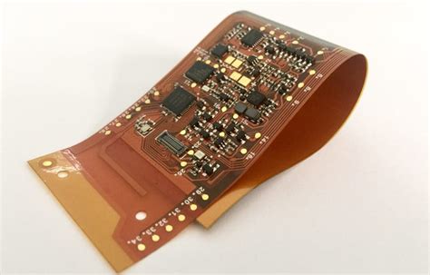
What is a Rigid-Flex PCB?
A Rigid-Flex PCB is a printed circuit board that combines both rigid and flexible substrates, allowing for a more compact and versatile design. This type of PCB consists of rigid sections, which provide structural support and house most of the components, and flexible sections, which enable the board to bend and fold, making it ideal for applications with limited space or unique packaging requirements.
Advantages of Rigid-Flex PCBs
- Space Savings: Rigid-Flex PCBs allow for a more compact design by eliminating the need for connectors and cables between rigid sections.
- Increased Reliability: By reducing the number of interconnects, Rigid-Flex PCBs minimize potential points of failure, resulting in higher reliability.
- Improved Signal Integrity: The continuous substrate of a Rigid-Flex PCB reduces signal loss and interference compared to traditional cable connections.
- Enhanced Design Flexibility: The ability to bend and fold the PCB enables designers to create unique form factors and accommodate unusual packaging constraints.
- Reduced Assembly Time: Rigid-Flex PCBs simplify the assembly process by eliminating the need for manual cable routing and connector assembly.
Rigid-Flex PCB Construction
A Rigid-Flex PCB is constructed by laminating together layers of flexible and rigid substrates, along with copper foil for the conductive traces. The most common materials used in Rigid-Flex PCB construction are:
| Material | Description |
|---|---|
| Polyimide | A flexible, heat-resistant polymer used as the base material for the flexible sections of the PCB |
| FR-4 | A rigid, glass-reinforced epoxy laminate used for the rigid sections of the PCB |
| Copper | A conductive metal used for the traces, pads, and vias |
| Coverlay | A protective layer applied to the flexible sections to insulate and protect the copper traces |
| Stiffeners | Added to the flexible sections to provide additional support and improve the PCB’s durability |
The manufacturing process for Rigid-Flex PCBs involves the following steps:
- Designing the PCB Layout, taking into account the placement of rigid and flexible sections
- Fabricating the flexible and rigid substrates separately
- Laminating the flexible and rigid layers together using heat and pressure
- Drilling and plating through-holes and vias
- Patterning and etching the copper traces
- Applying solder mask and silkscreen
- Cutting the PCB to its final shape

Rigid-Flex PCB Design Considerations
When designing a Rigid-Flex PCB, engineers must take into account several key factors to ensure optimal performance and reliability:
Bend Radius
The bend radius is the minimum radius at which the flexible section of the PCB can be bent without causing damage to the copper traces or the substrate. The bend radius is determined by the thickness and material properties of the flexible substrate, as well as the copper thickness. A general rule of thumb is to maintain a bend radius of at least 10 times the total thickness of the flexible section.
Flex-to-Rigid Transition
The transition point between the flexible and rigid sections of the PCB is a critical area that requires careful design consideration. To minimize stress on the copper traces and prevent delamination, it is essential to use a gradual transition with a small angle (usually less than 30 degrees). Additionally, copper traces should be routed perpendicular to the transition line to reduce the risk of cracking.
Stiffener Placement
Stiffeners are used to provide additional support to the flexible sections of the PCB and to prevent excessive bending. The placement of stiffeners should be carefully considered to ensure that they do not interfere with the desired bending profile of the PCB. Stiffeners are typically placed near connectors, components, and transition points.
Copper Thickness
The thickness of the copper traces in the flexible sections of the PCB should be carefully selected to balance flexibility and current-carrying capacity. Thinner copper traces (typically 0.5 oz or 17.5 μm) offer greater flexibility but have lower current-carrying capacity compared to thicker traces (1 oz or 35 μm). In some cases, a combination of thin and thick copper traces may be used to achieve the desired balance of flexibility and electrical performance.
Via Design
Vias in Rigid-Flex PCBs require special consideration to ensure reliability and prevent cracking during bending. Vias in the flexible sections should be designed with a smaller diameter and larger annular ring compared to those in the rigid sections. Additionally, the use of microvias and blind vias can help to minimize the stress on the flexible substrate.

Rigid-Flex PCB Applications
Rigid-Flex PCBs are used in a wide range of applications across various industries, including:
- Aerospace and Defense:
- Avionics systems
- Missile guidance systems
-
Satellite communication devices
-
Medical Devices:
- Wearable health monitors
- Implantable devices
-
Surgical instruments
-
Automotive:
- In-vehicle infotainment systems
- Advanced driver assistance systems (ADAS)
-
Engine control units (ECUs)
-
Consumer Electronics:
- Smartphones and tablets
- Smartwatches and fitness trackers
-
Virtual reality and augmented reality headsets
-
Industrial Automation:
- Robotics and motion control systems
- Machine vision systems
- Process control instrumentation

Rigid-Flex PCB Testing and Quality Control
To ensure the reliability and performance of Rigid-Flex PCBs, manufacturers employ various testing and quality control methods throughout the production process. Some of the most common tests include:
-
Visual Inspection: A visual examination of the PCB for defects such as misaligned layers, voids, or damage to the substrate or copper traces.
-
Continuity Testing: Verifying that all electrical connections are intact and that there are no shorts or open circuits.
-
Insulation Resistance (IR) Testing: Measuring the resistance between conductors to ensure adequate insulation and prevent leakage currents.
-
Time Domain Reflectometry (TDR) Testing: Analyzing the impedance and signal integrity of the PCB to identify any discontinuities or reflections.
-
Flexing and Bending Tests: Subjecting the PCB to repeated bending cycles to assess its durability and identify any potential weaknesses or failure points.
-
Thermal Cycling: Exposing the PCB to alternating high and low temperatures to simulate real-world operating conditions and verify its ability to withstand thermal stress.
-
Microsectioning: Cross-sectioning the PCB to examine the internal structure, layer alignment, and via integrity.
Rigid-Flex PCB Manufacturing Challenges and Solutions
Manufacturing Rigid-Flex PCBs presents unique challenges compared to traditional Rigid PCBs. Some of these challenges and their corresponding solutions include:
- Layer Alignment:
- Challenge: Ensuring accurate alignment of the flexible and rigid layers during lamination.
-
Solution: Use precision tooling and registration marks to maintain proper alignment throughout the manufacturing process.
-
Delamination:
- Challenge: Preventing delamination of the flexible and rigid layers, especially at the transition points.
-
Solution: Use a controlled lamination process with appropriate temperature, pressure, and duration, and design the transition points with a gradual angle.
-
Via Reliability:
- Challenge: Maintaining via integrity and preventing cracking during bending.
-
Solution: Use smaller via diameters, larger Annular rings, and microvias in the flexible sections, and fill vias with epoxy to improve mechanical strength.
-
Copper Cracking:
- Challenge: Preventing copper traces from cracking under repeated bending stress.
-
Solution: Use thinner copper traces in the flexible sections, route traces perpendicular to the bend line, and apply a strain relief coating to the traces.
-
Coverlay Adhesion:
- Challenge: Ensuring proper adhesion of the coverlay to the flexible substrate and copper traces.
- Solution: Use a compatible adhesive and controlled lamination process, and roughen the copper surface to improve adhesion.
FAQ
-
Q: What is the main difference between a Rigid-Flex PCB and a traditional rigid PCB?
A: A Rigid-Flex PCB combines both rigid and flexible substrates, allowing the board to bend and fold, while a traditional rigid PCB is composed entirely of rigid materials and cannot be bent. -
Q: What are the advantages of using a Rigid-Flex PCB over a rigid PCB with cable connections?
A: Rigid-Flex PCBs offer several advantages, including space savings, increased reliability, improved signal integrity, enhanced design flexibility, and reduced assembly time. -
Q: What materials are commonly used in the construction of Rigid-Flex PCBs?
A: The most common materials used in Rigid-Flex PCB construction are polyimide (flexible substrate), FR-4 (rigid substrate), copper (conductive traces), coverlay (protective layer), and stiffeners (for added support). -
Q: How does the bend radius affect the design of a Rigid-Flex PCB?
A: The bend radius determines the minimum radius at which the flexible section of the PCB can be bent without causing damage. It is typically recommended to maintain a bend radius of at least 10 times the total thickness of the flexible section. -
Q: What industries commonly use Rigid-Flex PCBs?
A: Rigid-Flex PCBs are used in various industries, including aerospace and defense, medical devices, automotive, consumer electronics, and industrial automation.
No responses yet