Introduction
The printed circuit board assembly (PCBA) process is a crucial stage in the electronics manufacturing industry, where individual electronic components are mounted and soldered onto a bare printed circuit board (PCB). This process transforms a bare PCB into a functional electronic assembly, ready for integration into various electronic devices and systems.
This comprehensive guideline will walk you through the step-by-step PCBA process, providing valuable insights into each stage and highlighting key considerations for successful assembly.
Step 1: PCB Preparation

1.1 PCB Inspection
Before initiating the assembly process, it is essential to thoroughly inspect the bare PCB for any defects or issues. This inspection can be performed visually or using automated optical inspection (AOI) systems. Common checks include:
- Alignment and registration of layers
- Presence of defects (shorts, opens, missing features)
- Surface finish quality
- Dimensional accuracy
Any defective PCBs should be identified and removed from the assembly process to ensure product quality and reliability.
1.2 Surface Treatment
Depending on the surface finish of the PCB, certain pre-treatment steps may be required to ensure proper solderability and component adhesion. Common surface treatments include:
- Plasma cleaning
- Chemical cleaning
- Brush scrubbing
- Baking (to remove moisture)
These treatments help remove contaminants, oxidation, and improve the wettability of the PCB surface for better solder joint formation.
Step 2: Solder Paste Application
2.1 Solder Paste Printing
Solder paste, a mixture of tiny solder spheres and flux, is applied to the PCB using a stencil printer. The stencil is carefully aligned with the PCB, and the solder paste is squeegeed through the apertures, depositing precise amounts onto the component pads and vias.
2.2 Solder Paste Inspection
After printing, the solder paste deposits are inspected for quality and consistency. Automated solder paste inspection (SPI) systems use various techniques, such as 3D imaging or laser triangulation, to ensure that the paste volume, height, and alignment meet the specified requirements.
Step 3: Component Placement
3.1 Component Preparation
Electronic components are prepared for placement, which may involve processes such as taping, forming, or trimming leads, depending on the component type and packaging.
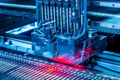
3.2 Pick-and-Place
Specialized pick-and-place machines are used to mount the components onto the PCB accurately. These machines use vision systems and programmable nozzles or grippers to pick up components from feeders and precisely place them onto the solder paste-covered pads.
3.3 Placement Inspection
After component placement, the PCB assembly undergoes an inspection to verify the correct positioning and orientation of the components. Automated optical inspection (AOI) systems or manual visual inspection methods can be employed for this purpose.
Step 4: Reflow Soldering
4.1 Reflow Oven
The populated PCB is passed through a reflow oven, where the solder paste is heated and melted, creating permanent electrical and mechanical connections between the components and the PCB.
4.2 Reflow Profile
The reflow process follows a carefully controlled temperature profile, which typically includes the following stages:
- Preheat: The PCB is gradually heated to activate the flux and prepare the solder paste for melting.
- Thermal Soak: A stable temperature is maintained to equalize the temperature across the PCB and components.
- Reflow: The temperature is raised above the melting point of the solder alloy, allowing the solder to melt and form solid joints upon cooling.
- Cooling: The PCB is cooled in a controlled manner to prevent defects and ensure proper solder joint formation.
4.3 Reflow Inspection
After the reflow process, the assembled PCB undergoes inspection to check for solder joint quality, component positioning, and potential defects. This can be done using automated X-ray inspection (AXI) or manual visual inspection methods.
Step 5: Cleaning and Conformal Coating (Optional)
5.1 Cleaning
Depending on the assembly requirements and the flux used, the assembled PCB may undergo a cleaning process to remove any residual flux or contaminants. Common cleaning methods include:
- Aqueous cleaning
- Semi-aqueous cleaning
- Vapor degreasing
- Inline cleaning
5.2 Conformal Coating
In applications where the PCB assembly will be exposed to harsh environments or requires additional protection, a conformal coating may be applied. This thin, protective layer helps prevent moisture, dust, and other contaminants from affecting the performance and reliability of the assembly.
Step 6: Final Inspection and Testing
6.1 Visual Inspection
A final visual inspection is performed to check for any visible defects, such as solder bridges, lifted leads, or missing components.
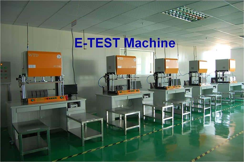
6.2 Functional Testing
Depending on the complexity of the assembly, various functional tests may be conducted to verify the overall performance and functionality of the PCB. These tests can include:
- In-circuit testing (ICT)
- Flying probe testing
- Boundary scan testing
- Functional testing (powered on)
6.3 Environmental Testing (Optional)
In certain applications, environmental testing may be required to ensure the PCB assembly’s reliability and performance under specific conditions. Common environmental tests include:
- Thermal cycling
- Vibration testing
- Humidity testing
- Salt spray testing
Step 7: Packaging and Shipping

7.1 Packaging
Once the assembled PCBs have passed all inspections and tests, they are carefully packaged for shipping or storage. Packaging materials and methods are chosen to provide adequate protection during transportation and handling.
7.2 Shipping
The packaged PCB assemblies are then shipped to the customer or the next stage of the manufacturing process, following appropriate shipping procedures and regulations.
Additional Considerations
1. Documentation and Traceability
Throughout the PCBA process, it is essential to maintain accurate documentation and traceability for quality control and compliance purposes. This includes recording data such as component batch numbers, process parameters, inspection results, and any deviations or non-conformances.
2. Electrostatic Discharge (ESD) Protection
Electronic components and PCB assemblies can be susceptible to damage from electrostatic discharge (ESD). Proper ESD-safe handling, work areas, and equipment are necessary to prevent potential failures and ensure product reliability.
3. Process Monitoring and Control
Continuous monitoring and control of the PCBA process parameters, such as temperatures, pressures, and timings, are crucial to ensure consistent quality and prevent defects. Statistical process control (SPC) techniques can be employed to monitor and improve the process.
4. Operator Training and Certification
Skilled and trained operators are essential for successful PCBA processes. Proper training and certification programs should be in place to ensure that operators are knowledgeable about the processes, equipment, and quality requirements.
5. Lean Manufacturing and Continuous Improvement
Implementing lean manufacturing principles and continuously improving the PCBA processes can lead to increased efficiency, reduced waste, and cost savings. Techniques such as value stream mapping, kaizen events, and root cause analysis can help identify and eliminate waste and inefficiencies.
Comparison Table: PCBA Process Steps and Considerations
To provide a concise overview of the PCBA process steps and associated considerations, the following table can be used:
| Step | Description | Key Considerations |
|---|---|---|
| 1. PCB Preparation | Inspection and surface treatment of bare PCB | Defect detection, surface finish quality |
| 2. Solder Paste Application | Printing and inspection of solder paste deposits | Solder paste volume, height, and alignment |
| 3. Component Placement | Preparation, pick-and-place, and inspection of components | Component positioning, orientation, and defects |
| 4. Reflow Soldering | Controlled heating and melting of solder paste | Reflow profile, solder joint quality, defects |
| 5. Cleaning and Conformal Coating (Optional) | Removal of flux residues, application of protective coating | Flux type, environmental protection requirements |
| 6. Final Inspection and Testing | Visual inspection, functional testing, environmental testing | Performance, reliability, compliance |
| 7. Packaging and Shipping | Protective packaging, transportation procedures | Handling, storage, shipping regulations |
Frequently Asked Questions (FAQ)
1. What is the typical cycle time for the PCBA process?
The cycle time for the PCBA process can vary significantly depending on factors such as the complexity of the assembly, the equipment used, and the production volume. Generally, cycle times can range from a few minutes to several hours for high-mix, low-volume assemblies, while high-volume production lines can achieve cycle times as low as a few seconds per assembly.
2. Can the PCBA process be fully automated?
While many steps in the PCBA process can be automated, such as solder paste printing, component placement, and reflow soldering, some manual intervention is often required for tasks like visual inspection, rework, and specialized testing. However, advances in automation and robotics are continuously increasing the level of automation possible in the PCBA process.
3. What are the most common defects encountered during the PCBA process?
Common defects encountered during the PCBA process include:
- Solder bridges (shorts between adjacent pads or components)
- Solder balls or splatters
- Lifted or misaligned components
- Insufficient or excessive solder paste deposition
- Flux residues or contamination
- Cold or dry solder joints
Effective inspection and quality control measures are crucial to identify and address these defects.
4. How does the component packaging (e.g., SMD, BGA, through-hole) affect the PCBA process?
The component packaging can significantly impact the PCBA process. Surface-mount components (SMDs) require different handling, placement, and soldering techniques compared to through-hole components. Additionally, advanced packages like ball grid arrays (BGAs) or chip-scale packages (CSPs) may require specialized equipment, reflow profiles, and inspection methods due to their unique form factors and high pin counts.
5. What are the key factors affecting the quality and reliability of PCBA assemblies?
Several factors contribute to the quality and reliability of PCBA assemblies, including:
- Component quality and adherence to specifications
- Accuracy of component placement and solder joint formation
- Cleanliness and absence of contaminants
- Proper reflow profile and temperature control
- Environmental protection (e.g., conformal coating)
- Rigorous inspection and testing procedures
- Handling and storage conditions
- Operator training and process control
Addressing these factors through robust processes, quality management systems, and continuous improvement efforts is essential for producing high-quality and reliable PCBA assemblies.
No responses yet