Introduction to PCB Phototools
Printed Circuit Boards (PCBs) are essential components in modern electronics, forming the backbone of countless devices we use every day. The process of creating these intricate designs involves several steps, one of which is the transfer of the PCB layout onto the copper-clad board. This is where PCB phototools come into play. In this comprehensive article, we will delve into the world of PCB phototools, exploring their importance, types, and the process of utilizing them for precise and efficient PCB image transfer.
What are PCB Phototools?
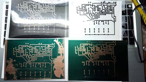
PCB phototools, also known as photomasks or artwork films, are transparent sheets containing the PCB layout design. These tools are used in the photolithography process to transfer the circuit pattern onto the photoresist-coated copper layer of the PCB. The dark areas of the phototool block the UV light, while the clear areas allow the light to pass through, exposing the photoresist and creating the desired pattern.
Importance of PCB Phototools
The accuracy and precision of PCB phototools are crucial for the successful fabrication of PCBs. Here are some key reasons why phototools are essential:
- High Resolution: Phototools enable the transfer of intricate designs with fine features and tight tolerances, ensuring the PCB functions as intended.
- Consistency: By using phototools, manufacturers can achieve consistent results across multiple PCB production runs, minimizing variations and defects.
- Cost-effective: Phototools offer a cost-effective solution for PCB Prototyping and small-scale production, as they eliminate the need for expensive direct imaging equipment.
Types of PCB Phototools
There are several types of PCB phototools available, each with its own characteristics and applications. Let’s explore the most common ones:
1. Film Phototools
Film phototools are the most widely used type in the PCB industry. They are created by printing the PCB layout onto a transparent film using a high-resolution plotter or imagesetter. The film is typically made of polyester or acetate material, which offers good dimensional stability and transparency.
Advantages of film phototools:
– Cost-effective for small to medium-scale production
– Easy to handle and store
– Compatible with various exposure systems
Disadvantages of film phototools:
– Limited resolution compared to glass phototools
– Susceptible to scratches and contamination
2. Glass Phototools
Glass phototools are high-precision masks created by etching the PCB layout onto a glass substrate coated with a thin layer of chrome. The chrome layer is selectively removed to create the desired pattern, resulting in a highly accurate and durable phototool.
Advantages of glass phototools:
– Exceptional resolution and accuracy
– Durable and resistant to wear and tear
– Ideal for high-volume production and fine-pitch designs
Disadvantages of glass phototools:
– Higher cost compared to film phototools
– Requires specialized equipment for production
– More fragile and prone to breakage if mishandled
3. Laser-printed Phototools
Laser-printed phototools are created using high-resolution laser printers on transparency films. While not as common as film or glass phototools, they offer a quick and affordable option for prototyping and low-volume production.
Advantages of laser-printed phototools:
– Fast and convenient production
– Low cost for small quantities
– Suitable for less demanding designs
Disadvantages of laser-printed phototools:
– Lower resolution compared to film and glass phototools
– Limited durability and reusability
– Not recommended for high-precision or high-volume applications
The PCB Image Transfer Process
Now that we’ve covered the types of PCB phototools let’s walk through the steps involved in using them for PCB image transfer.
Step 1: PCB Design and Phototool Preparation
The first step is to create the PCB layout using electronic design automation (EDA) software. Once the design is finalized, the artwork files are generated, typically in Gerber format. These files are then used to produce the phototool, either by printing on film or etching on glass, depending on the chosen type.
Step 2: Cleaning and Preparation of the Copper-clad Board
Before the image transfer process, the copper-clad board must be thoroughly cleaned to remove any contaminants or oxides that may affect the adhesion of the photoresist. This is usually done by scrubbing the board with an abrasive cleaner and then rinsing it with water and drying it completely.
Step 3: Photoresist Application
The cleaned copper-clad board is then coated with a thin layer of photoresist, a light-sensitive material that hardens when exposed to UV light. The photoresist can be applied using various methods, such as spin coating, spray coating, or dip coating, depending on the size and complexity of the board.
Step 4: Phototool Alignment and Exposure
Once the photoresist is applied, the phototool is carefully aligned with the copper-clad board, ensuring proper registration of the circuit pattern. The aligned phototool and board are then placed in an exposure unit, where UV light is used to transfer the pattern onto the photoresist. The exposure time depends on factors such as the type of photoresist, the intensity of the UV light, and the density of the phototool.
Step 5: Development and Etching
After exposure, the board is developed using a chemical solution that dissolves the unexposed areas of the photoresist, revealing the copper layer beneath. The developed board is then etched using a chemical etchant, typically ferric chloride or ammonium persulfate, which removes the exposed copper, leaving behind the desired circuit pattern.
Step 6: Stripping and Finishing
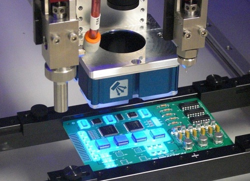
Finally, the remaining photoresist is stripped off the board using a solvent or an alkaline solution. The board may then undergo additional finishing processes, such as tin plating, solder mask application, and silkscreen printing, depending on the specific requirements of the PCB.

Advantages of Using PCB Phototools
Using PCB phototools for image transfer offers several advantages over other methods, such as direct printing or milling. Here are some key benefits:
- High Accuracy: Phototools enable the transfer of fine features and intricate designs with exceptional accuracy, ensuring the PCB functions as intended.
- Consistency: By using phototools, manufacturers can achieve consistent results across multiple PCB production runs, minimizing variations and defects.
- Scalability: Phototools are suitable for both prototyping and high-volume production, allowing for easy scaling of PCB manufacturing.
- Cost-effective: For small to medium-scale production, phototools offer a cost-effective solution compared to direct imaging or maskless lithography systems.
Challenges and Considerations
While PCB phototools are widely used and offer numerous benefits, there are some challenges and considerations to keep in mind:
- Resolution Limitations: The resolution of the phototool directly impacts the minimum feature size and spacing that can be achieved on the PCB. Film phototools have lower resolution compared to glass phototools, which may limit their use in high-density designs.
- Phototool Quality: The quality of the phototool is crucial for achieving accurate image transfer. Defects, scratches, or contamination on the phototool can lead to imperfections in the final PCB.
- Alignment and Registration: Proper alignment and registration of the phototool with the copper-clad board are essential for accurate image transfer. Misalignment can result in shifted or distorted circuit patterns.
- Environmental Control: The PCB image transfer process is sensitive to environmental factors such as temperature, humidity, and dust. Maintaining a controlled environment is necessary to ensure consistent results and minimize defects.
Frequently Asked Questions (FAQ)
- What is the difference between film and glass phototools?
Film phototools are created by printing the PCB layout onto a transparent film, while glass phototools are made by etching the layout onto a chrome-coated glass substrate. Glass phototools offer higher resolution and durability compared to film phototools but are more expensive and fragile. - Can I use a regular printer to create PCB phototools?
While it is possible to use a high-resolution laser printer to create phototools for less demanding designs, it is not recommended for high-precision or high-volume applications. For best results, use specialized plotters or imagesetters designed for phototool production. - How do I choose the right type of phototool for my PCB project?
The choice of phototool depends on factors such as the required resolution, feature size, production volume, and budget. Film phototools are suitable for most standard PCB designs, while glass phototools are recommended for high-density, fine-pitch designs, or high-volume production. - What is the typical resolution of PCB phototools?
The resolution of PCB phototools varies depending on the type. Film phototools typically have a resolution of around 8,000 to 20,000 dpi (dots per inch), while glass phototools can achieve resolutions of up to 50,000 dpi or higher. - How can I ensure the best results when using PCB phototools?
To ensure the best results, follow these guidelines: - Use high-quality phototools with the appropriate resolution for your design.
- Maintain a clean and controlled environment during the image transfer process.
- Ensure proper alignment and registration of the phototool with the copper-clad board.
- Follow the recommended exposure times and development procedures for your specific photoresist and equipment.
Conclusion
PCB phototools play a critical role in the PCB manufacturing process, enabling the accurate and consistent transfer of circuit patterns onto the copper-clad board. By understanding the types of phototools available and the image transfer process, PCB designers and manufacturers can choose the most suitable option for their specific requirements. While challenges exist, the use of high-quality phototools and adherence to best practices can ensure successful PCB fabrication and minimize defects. As PCB technology continues to advance, the importance of precise and reliable image transfer methods, such as those offered by phototools, will remain paramount in the production of high-quality, functional printed circuit boards.
No responses yet