Introduction to PCB Prototypes
PCB prototypes are an essential part of the electronics design and manufacturing process. They allow engineers and designers to test and validate their designs before committing to large-scale production. PCB prototypes are typically manufactured in small quantities, usually 3-5 pieces, to minimize costs and reduce the risk of design errors.
In this article, we will explore the process of manufacturing and assembling PCB prototypes, with a focus on the popular 3+3 prototype package. We will cover the various steps involved, from design to fabrication to assembly, and discuss the benefits and challenges of prototyping PCBs.
What are PCB Prototypes?
PCB prototypes are pre-production versions of printed circuit boards that are used for testing and validation purposes. They are designed to closely resemble the final product, but may have some differences in terms of materials, components, or manufacturing processes.
The main purpose of PCB prototypes is to:
- Test the functionality and performance of the circuit design
- Verify the accuracy of the PCB layout and component placement
- Identify and fix any design errors or issues before mass production
- Evaluate the manufacturability and assembly process of the PCB
- Demonstrate the product to stakeholders and potential customers
PCB prototypes are an important step in the product development lifecycle, as they help to reduce the risk of costly mistakes and delays in the later stages of production.

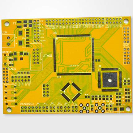
The 3+3 PCB Prototype Package
The 3+3 PCB prototype package is a popular option for many electronics designers and manufacturers. It typically includes:
- 3 bare PCBs (without components)
- 3 assembled PCBs (with components soldered)
The bare PCBs are used for testing the PCB fabrication process and checking the quality of the PCB materials and finishes. The assembled PCBs are used for testing the functionality and performance of the complete circuit.
The 3+3 package provides a good balance between cost and risk mitigation. It allows for sufficient testing and validation, while keeping the prototype quantity and costs relatively low.

PCB Prototype Design Considerations
Before starting the PCB Prototyping process, there are several design considerations that need to be taken into account. These include:
PCB Size and Thickness
The size and thickness of the PCB prototype should match the intended final product as closely as possible. This ensures that the prototype accurately represents the form factor and mechanical properties of the end product.
Common PCB sizes and thicknesses include:
| PCB Size | Dimensions (mm) | Thickness (mm) |
|---|---|---|
| Small | 50 x 50 | 0.8 – 1.6 |
| Medium | 100 x 100 | 1.6 – 2.0 |
| Large | 200 x 150 | 2.0 – 3.2 |
PCB Material Selection
The choice of PCB material depends on the electrical, thermal, and mechanical requirements of the circuit. Common PCB materials include:
- FR-4: A low-cost, general-purpose material suitable for most applications
- High Tg FR-4: An improved version of FR-4 with better thermal stability
- Rogers: A high-performance material with low dielectric loss and stable properties
- Aluminum: A metal-based material used for high-power and heat-sensitive applications
PCB Layer Stack-up
The number and arrangement of copper layers in the PCB stack-up affects the signal integrity, power delivery, and EMI performance of the circuit. A typical 4-layer PCB stack-up includes:
| Layer | Description |
|---|---|
| Top | Signal layer |
| Inner | Ground plane |
| Inner | Power plane |
| Bottom | Signal layer |
Component Selection and Placement
The selection and placement of components on the PCB prototype should follow best practices for manufacturability, reliability, and signal integrity. This includes:
- Choosing components with appropriate packages and footprints
- Placing components to minimize trace lengths and signal crosstalk
- Providing adequate clearances and spacing between components
- Considering the assembly process and orientation of components
PCB Prototype Fabrication Process
Once the PCB design is finalized, the next step is to fabricate the bare PCBs. The fabrication process typically involves the following steps:
PCB CAD/CAM
The PCB design files (Gerber, drill, and component data) are imported into a computer-aided design/manufacturing (CAD/CAM) system. The CAD/CAM software performs design rule checks (DRC) and generates the machine-readable files needed for fabrication.
PCB Printing and Etching
The copper layers of the PCB are printed and etched using a photolithography process. This involves:
- Applying a photoresist coating to the copper-clad laminate
- Exposing the photoresist to UV light through a photomask
- Developing the photoresist to remove the unexposed areas
- Etching away the unprotected copper using a chemical solution
- Stripping away the remaining photoresist
PCB Drilling and Routing
The PCB panel is drilled and routed to create the holes and outlines of the individual PCBs. This is done using computer-controlled drilling and routing machines.
PCB Plating and Finishing
The drilled holes are plated with copper to create electrical connections between layers. The PCB surface is then finished with a protective coating, such as solder mask, silkscreen, or gold/silver plating.
PCB Electrical Testing
The fabricated PCBs undergo electrical testing to ensure that they meet the specified requirements for continuity, insulation resistance, and high-potential (hipot) performance.
PCB Prototype Assembly Process
After the bare PCBs are fabricated, the next step is to assemble the components onto the boards. The assembly process typically involves the following steps:
Solder Paste Printing
A solder paste is applied to the PCB pads using a stencil printing process. The solder paste contains tiny solder particles suspended in a flux medium.
Component Placement
The components are placed onto the PCB pads using an automated pick-and-place machine. The machine uses computer vision and Robotic Arms to accurately place the components based on the CAD data.
Reflow Soldering
The PCB with the placed components is heated in a reflow oven to melt the solder paste and form a solid solder joint between the component leads and the PCB pads.
Inspection and Testing
The assembled PCBs are visually inspected and electrically tested to ensure that all components are properly soldered and functioning correctly.
Benefits of PCB Prototyping
PCB prototyping offers several benefits to electronics designers and manufacturers, including:
Risk Reduction
PCB prototypes help to identify and fix design errors early in the development process, reducing the risk of costly mistakes and delays in later stages of production.
Design Validation
PCB prototypes allow designers to test and validate the functionality, performance, and reliability of their designs before committing to large-scale production.
Faster Time-to-Market
By catching design issues early and iterating quickly, PCB prototyping can help to accelerate the product development timeline and bring products to market faster.
Cost Savings
PCB prototypes are typically less expensive than full production runs, allowing designers to experiment with different design options and optimize their designs for cost and manufacturability.
Challenges of PCB Prototyping
While PCB prototyping offers many benefits, there are also some challenges that designers and manufacturers need to be aware of, including:
Limited Quantity
PCB prototypes are typically manufactured in small quantities, which can limit the amount of testing and validation that can be performed.
Material and Process Differences
PCB prototypes may use different materials or manufacturing processes than the final production boards, which can affect the performance and reliability of the prototype.
Component Availability
Some components may be difficult or expensive to source in small quantities, which can impact the cost and lead time of the prototype.
Design Changes
If significant design changes are required after the prototype is built, it can be costly and time-consuming to fabricate new prototypes.
FAQ
How long does it take to manufacture a PCB prototype?
The lead time for PCB prototypes can vary depending on the complexity of the design and the fabrication process. Typically, a simple 2-layer PCB prototype can be manufactured in 1-2 weeks, while a complex multi-layer PCB may take 3-4 weeks or longer.
How much does a PCB prototype cost?
The cost of a PCB prototype depends on factors such as the PCB size, layer count, material, and quantity. As a rough estimate, a simple 2-layer PCB prototype may cost $50-$100 per piece, while a complex multi-layer PCB may cost several hundred dollars per piece.
What files are needed to manufacture a PCB prototype?
To manufacture a PCB prototype, you typically need to provide the following files to the fabrication house:
- Gerber files (copper layers, solder mask, silkscreen, drill data)
- Bill of Materials (BOM) with component information
- Assembly drawings or pick-and-place files
Can I assemble the PCB prototype myself?
Yes, it is possible to assemble the PCB prototype yourself if you have the necessary skills, tools, and equipment. However, for most designers, it is more cost-effective and time-efficient to outsource the assembly process to a professional assembly house.
What should I do if my PCB prototype doesn’t work?
If your PCB prototype doesn’t work as expected, the first step is to diagnose the issue. This may involve:
- Visual inspection of the PCB and components for any obvious defects or damage
- Continuity testing to check for open or short circuits
- Functional testing to isolate the faulty subsystem or component
- Comparing the prototype to the original design files to identify any discrepancies
Once the issue is identified, you may need to modify the design, replace components, or re-fabricate the PCB to fix the problem.
Conclusion
PCB prototyping is a critical step in the electronics design and manufacturing process. It allows designers to test and validate their designs, identify and fix issues early, and optimize their products for cost and manufacturability.
The 3+3 PCB prototype package is a popular option that provides a good balance between cost and risk mitigation. By carefully considering the design requirements, fabrication process, and assembly methods, designers can create high-quality PCB prototypes that accurately represent their final products.
While PCB prototyping has its challenges, the benefits of reduced risk, faster time-to-market, and cost savings make it an essential part of any successful electronics project. By following best practices and working with experienced fabrication and assembly partners, designers can unlock the full potential of PCB prototyping and bring their innovative products to life.
No responses yet