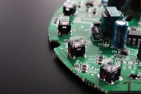
PCB Components
Substrate
The substrate is the foundation of a PCB, providing a stable and insulating base for the conductive traces and components. The most common substrate materials are:
- FR-4 (Flame Retardant 4): A glass-reinforced epoxy laminate, FR-4 is the most widely used substrate material due to its excellent mechanical and electrical properties, as well as its cost-effectiveness.
- High-Frequency Materials: For applications requiring high-frequency performance, such as RF and microwave circuits, specialized substrate materials like Rogers RO4000 series, Teflon, and ceramic-based substrates are used.
- Flexible Substrates: Flexible PCBs use thin, flexible materials like polyimide (Kapton) or polyester as substrates, allowing the board to bend and conform to various shapes.
Copper Foil
Copper foil is the conductive layer that forms the traces, pads, and planes on a PCB. The foil is typically available in thicknesses ranging from 0.5 oz to 2 oz per square foot (17 to 70 μm). The choice of foil thickness depends on the current-carrying requirements and the desired trace width and spacing.
Solder Mask
Solder mask is a protective layer applied over the copper traces, leaving only the exposed pads and areas intended for soldering. It prevents solder bridges and short circuits during the assembly process. Solder mask is typically green in color but is also available in other colors like red, blue, and black.
Silkscreen
Silkscreen is a printed layer on top of the solder mask that provides text, logos, and component identifiers. It helps in the assembly and troubleshooting of the PCB. White is the most common silkscreen color, but other colors are available as well.
Surface Finish
The surface finish is applied to the exposed copper pads to prevent oxidation and enhance solderability. Some common surface finishes include:
- HASL (Hot Air Solder Leveling): A tin-lead alloy is applied to the pads and then leveled using hot air.
- ENIG (Electroless Nickel Immersion Gold): A layer of nickel is deposited on the pads, followed by a thin layer of gold.
- OSP (Organic Solderability Preservative): A thin, organic coating is applied to the pads to protect them from oxidation.
PCB Material Properties
When selecting materials for PCB Fabrication, several key properties must be considered:
Dielectric Constant (Dk)
The dielectric constant is a measure of a material’s ability to store electrical energy. A lower Dk value indicates better signal integrity and higher-frequency performance. FR-4 has a Dk value of around 4.2 at 1 MHz, while high-frequency materials like Rogers RO4350B have a Dk of 3.48 at 10 GHz.
Dissipation Factor (Df)
The dissipation factor, also known as loss tangent, represents the amount of energy lost as heat when an alternating electric field is applied to the material. A lower Df value is desirable for high-frequency applications. FR-4 has a Df value of around 0.02 at 1 MHz, while Rogers RO4350B has a Df of 0.0037 at 10 GHz.
Thermal Conductivity
Thermal conductivity is a measure of a material’s ability to conduct heat. Higher thermal conductivity helps in dissipating heat generated by components, preventing thermal damage and improving reliability. FR-4 has a thermal conductivity of around 0.3 W/mK, while aluminum-based PCBs can have thermal conductivities up to 150 W/mK.
CTE (Coefficient of Thermal Expansion)
CTE indicates how much a material expands or contracts with changes in temperature. A mismatch in CTE between the PCB Substrate and components can lead to mechanical stress and failures. FR-4 has a CTE of around 14 ppm/°C in the X-Y plane and 50 ppm/°C in the Z-axis.
Advanced PCB Materials
As technology advances and the demand for high-performance electronics grows, new PCB materials are being developed to meet these challenges:
High-Speed Materials
For applications requiring high-speed data transmission, such as 5G networks and high-performance computing, low-loss materials with tight Dk and Df control are essential. Some examples include Isola’s Tachyon 100G and Rogers’ CLTE series.
Thermally Conductive Materials
To address the increasing power densities in modern electronics, thermally conductive PCB materials are being developed. These materials incorporate fillers like ceramics or carbon fibers to enhance thermal conductivity. Examples include Ventec’s VT-4B5 and Arlon’s 85-MT.
Embedded Components
Embedding components within the PCB substrate can save space, reduce parasitic effects, and improve performance. Materials like Isola’s Astra MT77 and 3M’s ECF (Embedded Capacitor Film) enable the integration of passive components within the PCB stack-up.

PCB Material Selection Considerations
When choosing materials for a PCB, several factors must be considered:
- Electrical Requirements: Consider the operating frequency, signal integrity, and power handling requirements of the application.
- Environmental Conditions: Take into account the temperature range, humidity, and exposure to chemicals or other harsh conditions.
- Mechanical Requirements: Evaluate the need for flexibility, rigidity, and resistance to vibration or shock.
- Cost and Availability: Balance the performance requirements with the cost and availability of the materials.
- Manufacturing Capabilities: Ensure that the chosen materials are compatible with the available manufacturing processes and equipment.

Frequently Asked Questions (FAQ)
1. What is the most commonly used PCB substrate material?
FR-4 (Flame Retardant 4) is the most widely used PCB substrate material due to its good mechanical and electrical properties, as well as its cost-effectiveness.
2. What are the main components of a PCB?
The main components of a PCB are the substrate, copper foil, solder mask, silkscreen, and surface finish.
3. What is the purpose of solder mask on a PCB?
Solder mask is a protective layer applied over the copper traces, leaving only the exposed pads and areas intended for soldering. It prevents solder bridges and short circuits during the assembly process.
4. What is the difference between HASL and ENIG surface finishes?
HASL (Hot Air Solder Leveling) is a tin-lead alloy applied to the pads and leveled using hot air, while ENIG (Electroless Nickel Immersion Gold) consists of a layer of nickel deposited on the pads, followed by a thin layer of gold.
5. What factors should be considered when selecting materials for a PCB?
When choosing materials for a PCB, consider the electrical requirements, environmental conditions, mechanical requirements, cost and availability, and manufacturing capabilities.
| Property | FR-4 | Rogers RO4350B |
|---|---|---|
| Dielectric Constant (Dk) at 1 MHz | 4.2 | – |
| Dielectric Constant (Dk) at 10 GHz | – | 3.48 |
| Dissipation Factor (Df) at 1 MHz | 0.02 | – |
| Dissipation Factor (Df) at 10 GHz | – | 0.0037 |
| Thermal Conductivity (W/mK) | 0.3 | 0.62 |
| CTE (ppm/°C) in X-Y plane | 14 | 11 |
| CTE (ppm/°C) in Z-axis | 50 | 32 |
Table 1: Comparison of key properties between FR-4 and Rogers RO4350B PCB materials.
In conclusion, understanding the basic components and materials used in PCB fabrication is essential for designing and manufacturing reliable and high-performance electronic devices. By carefully considering the electrical, thermal, and mechanical requirements of an application, and selecting the appropriate materials, designers can ensure optimal PCB performance and longevity.
No responses yet