
Mistake 1: Inadequate Planning and Design Validation
One of the most common mistakes in PCB design is inadequate planning and design validation. Before starting the design process, it is essential to have a clear understanding of the project requirements, including the functionality, form factor, and performance specifications. Designers should also consider the manufacturing capabilities and constraints of the PCB fabricator and assembler.
Tips to avoid this mistake:
- Create a detailed design specification document that outlines all the project requirements and constraints.
- Use simulation tools to validate the design before proceeding to the physical layout.
- Collaborate with the PCB fabricator and assembler to ensure that the design is manufacturable and meets their capabilities.
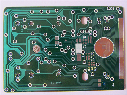
Mistake 2: Incorrect Component Placement and Orientation
Incorrect component placement and orientation can lead to signal integrity issues, thermal problems, and manufacturing difficulties. Designers should consider the component size, shape, and pin configuration when placing them on the board. They should also ensure that the components are oriented correctly to avoid assembly errors.
Tips to avoid this mistake:
- Use a component library that includes accurate footprints and 3D models of the components.
- Follow the manufacturer’s recommended placement and orientation guidelines for each component.
- Use design rule checks (DRC) to ensure that the component placement meets the design constraints.
Mistake 3: Inadequate Grounding and Power Distribution
Inadequate grounding and power distribution can lead to signal integrity issues, electromagnetic interference (EMI), and power supply noise. Designers should create a robust power and ground plane that provides a low-impedance path for the current flow. They should also use appropriate decoupling capacitors to reduce power supply noise and ensure that the power is distributed evenly across the board.
Tips to avoid this mistake:
- Use a dedicated power and ground plane for each voltage level.
- Place decoupling capacitors close to the power pins of the components.
- Use via stitching to create a low-impedance path between the power and ground planes.

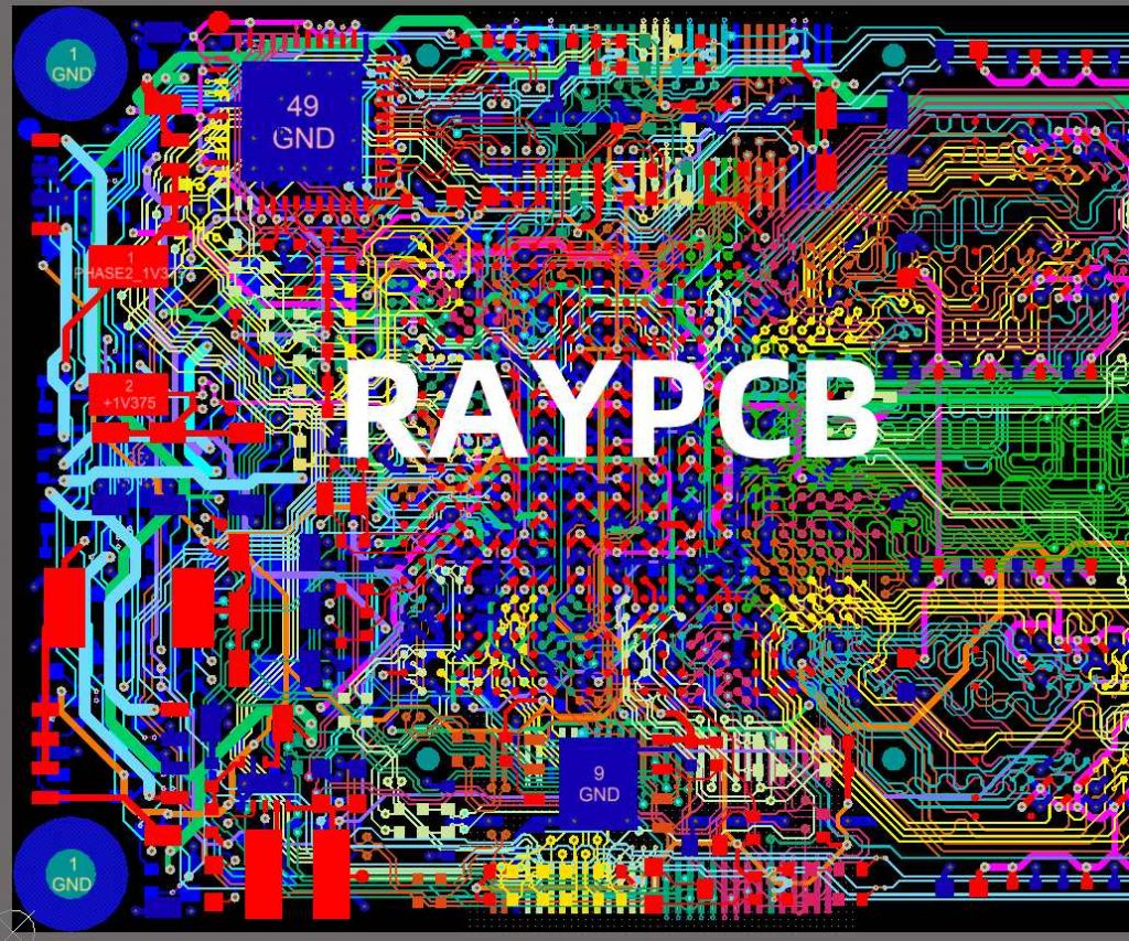
Mistake 4: Incorrect Trace Routing and Spacing
Incorrect trace routing and spacing can lead to signal integrity issues, crosstalk, and EMI. Designers should follow the PCB design guidelines for trace width, spacing, and impedance matching. They should also consider the signal speed and frequency when routing the traces to avoid reflections and ringing.
Tips to avoid this mistake:
- Use a PCB design tool that supports impedance matching and automatically calculates the trace width and spacing based on the signal requirements.
- Route high-speed signals on the outer layers of the board to minimize the dielectric losses and crosstalk.
- Use ground planes or guard traces to isolate sensitive signals from noisy ones.
Mistake 5: Inadequate Documentation and Version Control
Inadequate documentation and version control can lead to confusion, errors, and delays in the manufacturing process. Designers should create a comprehensive documentation package that includes the schematic, layout, bill of materials (BOM), and assembly instructions. They should also use a version control system to track the changes and revisions of the design files.
Tips to avoid this mistake:
- Create a documentation template that includes all the necessary information for manufacturing and assembly.
- Use a version control system such as Git or SVN to track the changes and revisions of the design files.
- Collaborate with the manufacturing team to ensure that the documentation is clear and complete.
FAQ
Q1: What is the importance of PCB design in electronic product development?
A1: PCB design is crucial in electronic product development as it determines the functionality, reliability, and manufacturability of the final product. A well-designed PCB can reduce the overall cost, improve the performance, and accelerate the time-to-market of the product.
Q2: What are some common PCB Design Mistakes that should be avoided?
A2: Some common PCB design mistakes include inadequate planning and design validation, incorrect component placement and orientation, inadequate grounding and power distribution, incorrect trace routing and spacing, and inadequate documentation and version control.
Q3: How can designers ensure that their PCB design is manufacturable?
A3: Designers can ensure that their PCB design is manufacturable by collaborating with the PCB fabricator and assembler, following the design guidelines and constraints, using simulation tools to validate the design, and creating a comprehensive documentation package.
Q4: What are some best practices for trace routing and spacing in PCB design?
A4: Some best practices for trace routing and spacing in PCB design include using a PCB design tool that supports impedance matching and automatically calculates the trace width and spacing based on the signal requirements, routing high-speed signals on the outer layers of the board to minimize the dielectric losses and crosstalk, and using ground planes or guard traces to isolate sensitive signals from noisy ones.
Q5: What is the importance of documentation and version control in PCB design?
A5: Documentation and version control are essential in PCB design to ensure that the manufacturing process runs smoothly and efficiently. A comprehensive documentation package that includes the schematic, layout, BOM, and assembly instructions can reduce errors and delays in the manufacturing process. Version control systems can help track the changes and revisions of the design files and ensure that everyone is working with the latest version of the design.
| Mistake | Tips to Avoid |
|---|---|
| Inadequate Planning and Design Validation | Create a detailed design specification document, use simulation tools to validate the design, collaborate with the PCB fabricator and assembler. |
| Incorrect Component Placement and Orientation | Use a component library with accurate footprints and 3D models, follow the manufacturer’s recommended placement and orientation guidelines, use design rule checks. |
| Inadequate Grounding and Power Distribution | Use a dedicated power and ground plane for each voltage level, place decoupling capacitors close to the power pins of the components, use via stitching. |
| Incorrect Trace Routing and Spacing | Use a PCB design tool that supports impedance matching and automatically calculates the trace width and spacing, route high-speed signals on the outer layers, use ground planes or guard traces to isolate sensitive signals. |
| Inadequate Documentation and Version Control | Create a documentation template that includes all the necessary information for manufacturing and assembly, use a version control system, collaborate with the manufacturing team. |
In conclusion, PCB design is a critical aspect of electronic product development that requires careful planning, attention to detail, and adherence to best practices. By avoiding common mistakes such as inadequate planning and design validation, incorrect component placement and orientation, inadequate grounding and power distribution, incorrect trace routing and spacing, and inadequate documentation and version control, designers can create high-quality PCBs that meet the project requirements and are manufacturable and reliable. By following the tips and best practices outlined in this article, designers can minimize the risk of costly reworks, delays, and product failures, and accelerate the time-to-market of their electronic products.
No responses yet