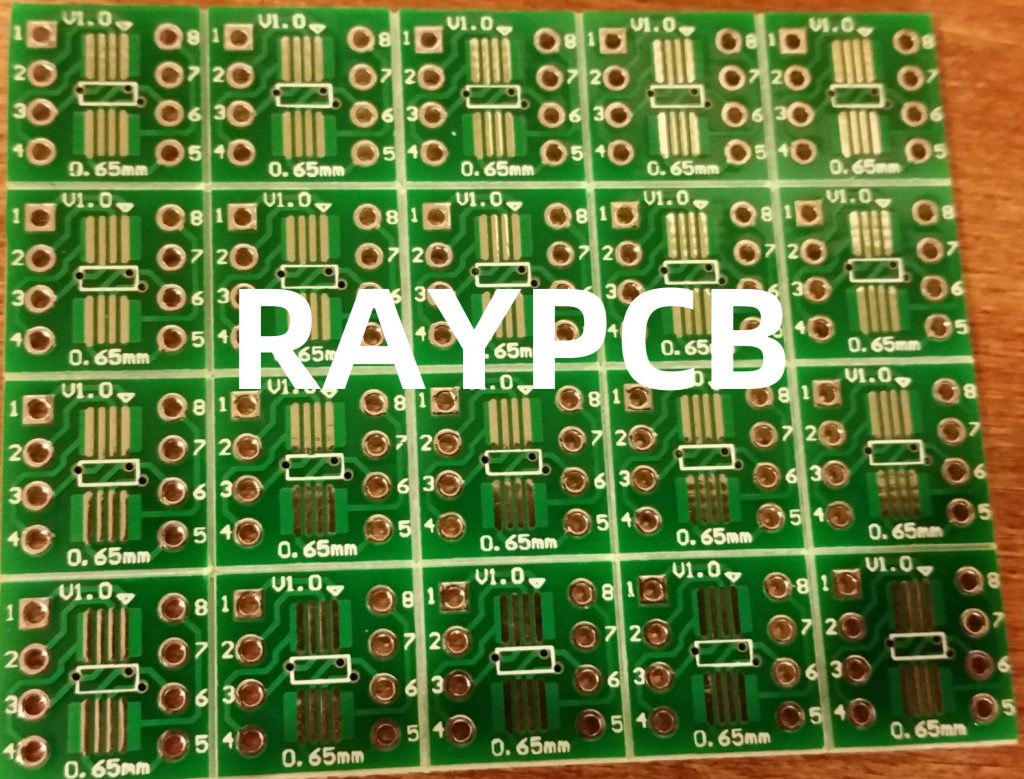
What is a PCB?
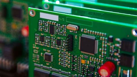
A Printed Circuit Board (PCB) is a thin board made of fiberglass or composite material that has conductive pathways printed or etched onto its surface. These pathways, called traces, connect various points on the board electrically. PCBs are used to mechanically support and electrically connect electronic components using conductive tracks, pads, and other features.
Key Components of a PCB
- Substrate: The base material of the PCB, typically made of fiberglass or composite material.
- Copper Layers: Thin layers of copper foil laminated onto the substrate. These layers are etched to create the conductive pathways.
- Solder Mask: A protective layer applied over the copper traces to prevent short circuits and provide insulation.
- Silkscreen: A printed layer on top of the solder mask used for labeling components, test points, and other information.
- Vias: Small holes drilled through the board to connect traces on different layers.
- Pads: Exposed areas of copper used for soldering components to the board.
Types of PCBs
PCBs can be classified based on the number of layers, the material used, and their purpose. Here are some common types of PCBs:
Single-Sided PCBs
Single-sided PCBs have conductive traces on only one side of the substrate. They are the simplest and most cost-effective type of PCB but have limitations in terms of circuit complexity and density.
Double-Sided PCBs
Double-sided PCBs have conductive traces on both sides of the substrate. They offer higher circuit density and more flexibility in design compared to single-sided PCBs. The two sides are connected using vias.
Multi-Layer PCBs
Multi-layer PCBs have three or more conductive layers separated by insulating layers. They offer the highest circuit density and are used in complex electronic devices. The layers are interconnected using vias.
| PCB Type | Layers | Cost | Complexity | Applications |
|---|---|---|---|---|
| Single-Sided | 1 | Low | Low | Simple devices, prototypes |
| Double-Sided | 2 | Medium | Medium | Moderately complex devices |
| Multi-Layer | 3+ | High | High | Complex devices, high-density applications |
Rigid PCBs
Rigid PCBs are made using a solid substrate material, typically fiberglass. They are the most common type of PCB and are used in a wide range of applications.
Flexible PCBs
Flexible PCBs (FPCBs) are made using a flexible substrate material, such as polyimide. They can be bent, twisted, or folded to fit into tight spaces or conform to a specific shape. FPCBs are commonly used in wearable devices, medical equipment, and aerospace applications.
Rigid-Flex PCBs
Rigid-flex PCBs combine the benefits of both rigid and flexible PCBs. They consist of rigid sections connected by flexible sections, allowing for three-dimensional designs and improved reliability in applications with limited space or demanding mechanical requirements.
PCB Manufacturing Process
The PCB manufacturing process involves several steps, each requiring precision and attention to detail. Here’s a brief overview of the process:
- Design: The PCB design is created using specialized software, such as EDA (Electronic Design Automation) tools. The design includes the schematic, component placement, and routing of the conductive traces.
- Printing: The design is printed onto a transparent film or directly onto the copper-clad substrate using a photoplotter or direct imaging process.
- Etching: The exposed copper is etched away using a chemical solution, leaving only the desired conductive traces.
- Lamination: For multi-layer PCBs, the individual layers are aligned and laminated together under heat and pressure.
- Drilling: Holes are drilled through the board for component leads, vias, and mounting.
- Plating: The holes are plated with copper to ensure electrical connectivity between layers.
- Solder Mask Application: A solder mask is applied to protect the copper traces and prevent short circuits.
- Silkscreen Printing: The silkscreen layer is printed onto the solder mask for labeling and identification.
- Surface Finish: A surface finish, such as HASL (Hot Air Solder Leveling) or ENIG (Electroless Nickel Immersion Gold), is applied to protect the exposed copper and improve solderability.
- Cutting and Routing: The panel containing multiple PCBs is cut and routed into individual boards.
- Quality Control: The finished PCBs undergo rigorous testing and inspection to ensure they meet the required specifications and standards.

PCB Design Considerations
Designing a PCB involves several key considerations to ensure optimal performance, reliability, and manufacturability. Some of these considerations include:
Component Placement
Components should be placed in a logical and efficient manner, taking into account factors such as signal integrity, thermal management, and mechanical constraints. Proper component placement can minimize the length of traces, reduce electromagnetic interference (EMI), and improve overall system performance.
Trace Width and Spacing
The width and spacing of the conductive traces on a PCB must be carefully designed to ensure proper signal integrity and prevent crosstalk. Factors such as the required current carrying capacity, impedance matching, and the manufacturing capabilities of the PCB fabricator must be considered when determining trace width and spacing.
Via Design
Vias are used to interconnect traces on different layers of a multi-layer PCB. The size, placement, and type of vias (e.g., through-hole, blind, or buried) must be carefully designed to ensure reliable electrical connections and minimize signal degradation.
Grounding and Power Distribution
Proper grounding and power distribution are critical for the performance and reliability of a PCB. A well-designed ground plane helps to minimize EMI and provides a stable reference for signals. Power distribution networks should be designed to provide adequate current to all components while minimizing voltage drop and noise.
Thermal Management
Electronic components generate heat during operation, which must be dissipated to prevent damage and ensure reliable performance. PCB designers must consider factors such as component power dissipation, ambient temperature, and available cooling methods when designing the thermal management system for a PCB.

PCB Testing and Inspection
Once a PCB has been manufactured, it must undergo rigorous testing and inspection to ensure it meets the required specifications and standards. Some common PCB testing and inspection methods include:
Visual Inspection
Visual inspection is the first step in PCB testing and involves examining the board for any obvious defects, such as missing components, solder bridges, or damaged traces. This can be done manually or using automated optical inspection (AOI) equipment.
Electrical Testing
Electrical testing involves verifying the electrical functionality of the PCB, including continuity, insulation resistance, and voltage levels. This can be done using a variety of test equipment, such as multimeters, oscilloscopes, and boundary scan testing systems.
Functional Testing
Functional testing involves verifying that the PCB performs its intended function when connected to the larger system or device. This can involve testing the board under various environmental conditions, such as temperature, humidity, and vibration, to ensure reliable performance in the intended application.
Burn-In Testing
Burn-in testing involves operating the PCB under elevated temperature and voltage conditions for an extended period to identify any early failures or defects. This helps to ensure that the board will perform reliably over its intended lifespan.
Frequently Asked Questions (FAQ)
What is the difference between a PCB and a PCBA?
A PCB (Printed Circuit Board) is the bare board without any components attached. A PCBA (Printed Circuit Board Assembly) is a PCB that has been populated with electronic components and is ready for use in an electronic device.
What are the advantages of using a PCB?
PCBs offer several advantages over other methods of electronic circuit construction, such as point-to-point wiring or wire-wrap. These advantages include:
- Reduced size and weight
- Improved reliability and durability
- Faster and more automated assembly
- Lower production costs for high-volume applications
- Easier troubleshooting and repair
What materials are PCBs made from?
PCBs are typically made from a combination of materials, including:
- Substrate material (e.g., fiberglass, composite)
- Copper foil for conductive traces
- Solder mask for insulation and protection
- Silkscreen for labeling and identification
- Surface finish (e.g., HASL, ENIG) for protection and improved solderability
What is the typical lifespan of a PCB?
The lifespan of a PCB depends on several factors, including the materials used, the manufacturing process, the environmental conditions, and the intended application. In general, a well-designed and manufactured PCB can last for several decades under normal operating conditions. However, factors such as high temperatures, humidity, vibration, and exposure to contaminants can significantly reduce the lifespan of a PCB.
How can I ensure the reliability and durability of my PCB design?
To ensure the reliability and durability of your PCB design, you should consider the following factors:
- Use high-quality materials and components
- Follow best practices for PCB design, including proper component placement, trace routing, and grounding
- Perform thorough testing and inspection during the manufacturing process
- Use appropriate protective measures, such as conformal coating or potting, for harsh environments
- Follow proper handling and storage procedures to prevent damage or contamination
- Design for manufacturability and testability to minimize defects and improve yield.
By carefully considering these factors and working closely with experienced PCB manufacturers and assemblers, you can ensure that your PCB design will provide reliable and durable performance in its intended application.
No responses yet