The Importance of PCB Assembly Inspections
PCB assembly inspections play a vital role in maintaining the quality, reliability, and performance of the final product. By identifying and addressing potential issues early in the manufacturing process, inspections help to minimize costly rework, reduce product failures, and improve overall customer satisfaction. Some of the key benefits of conducting thorough PCB assembly inspections include:
- Detecting and correcting defects early in the process
- Ensuring the functionality and reliability of the final product
- Reducing the risk of product failures and recalls
- Minimizing production delays and costs associated with rework
- Maintaining high quality standards and customer satisfaction
Types of PCB Assembly Inspections
In a one-stop PCB assembly process, multiple inspections are performed at various stages to ensure the quality and integrity of the PCBs. The following are the primary types of inspections conducted:
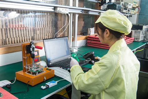
Visual Inspection
Visual inspection is the most basic and commonly used method of PCB assembly inspection. This process involves carefully examining the PCB using the naked eye or magnification tools to identify any visible defects or irregularities. Some of the aspects checked during visual inspection include:
- Component placement and orientation
- Solder joint quality
- Cleanliness of the PCB surface
- Presence of any foreign objects or debris
- Correct labeling and markings
Visual inspection is typically performed at multiple stages of the assembly process, including pre-assembly, post-soldering, and final inspection.
Automated Optical Inspection (AOI)
Automated Optical Inspection (AOI) is a more advanced and efficient method of PCB Inspection that utilizes high-resolution cameras and sophisticated software algorithms to detect defects and irregularities. AOI systems capture images of the PCB and compare them to a predefined set of criteria or a “golden board” to identify any deviations. Some of the defects that AOI systems can detect include:
- Missing, misaligned, or incorrect components
- Solder bridges, opens, or insufficient solder
- Lifted or tombstoned components
- Incorrect polarity or orientation of components
- Damaged or missing solder mask
AOI is typically performed immediately after the soldering process and can quickly inspect large volumes of PCBs, making it an essential tool for high-volume production.
X-ray inspection
X-ray inspection is a non-destructive testing method that uses X-rays to examine the internal structure of a PCB, particularly for components with hidden solder joints, such as ball grid arrays (BGAs) and quad flat no-lead (QFN) packages. X-ray inspection systems create a detailed image of the PCB, allowing technicians to identify defects that may not be visible through other inspection methods. Some of the aspects checked during X-ray inspection include:
- Solder joint quality and voids
- Correct alignment and placement of hidden components
- Presence of foreign objects or debris within the PCB
- Integrity of internal traces and connections
X-ray inspection is typically performed on a sample basis or for critical components that require a higher level of scrutiny.
In-Circuit Testing (ICT)
In-Circuit Testing (ICT) is a functional testing method that verifies the electrical connectivity and performance of individual components on a PCB. ICT systems use a bed-of-nails fixture to make contact with specific test points on the PCB and apply electrical signals to test the functionality of each component. Some of the aspects checked during ICT include:
- Correct component values (resistance, capacitance, inductance)
- Open or short circuits
- Correct diode and transistor functionality
- Presence of any missing or incorrect components
ICT is typically performed after the final assembly and before the final functional testing of the PCB.
Functional Testing
Functional testing is the final stage of PCB assembly inspection, where the fully assembLED PCB is tested to ensure it meets the specified performance requirements and functions as intended. This process involves powering up the PCB and running a series of tests to verify its operation under various conditions. Some of the aspects checked during functional testing include:
- Correct input/output functionality
- Proper communication between components
- Stable operation under different voltage and temperature conditions
- Absence of any intermittent or random failures
Functional testing is critical for ensuring that the PCB will perform reliably in its intended application and meet customer expectations.

Implementing PCB Assembly Inspections in One-Stop PCB Assembly
In a one-stop PCB assembly process, implementing a comprehensive inspection plan is essential for maintaining quality and efficiency throughout the manufacturing process. Some of the key considerations for implementing PCB assembly inspections in a one-stop facility include:
- Defining clear quality standards and acceptance criteria
- Investing in advanced inspection equipment and software
- Training personnel in the proper use of inspection tools and techniques
- Establishing a clear documentation and reporting system for inspection results
- Continuously monitoring and improving the inspection process based on feedback and data analysis
By incorporating thorough PCB assembly inspections at every stage of the manufacturing process, one-stop PCB assembly providers can ensure the highest level of quality and reliability for their customers.

Conclusion
PCB assembly inspections are a critical component of the one-stop PCB assembly process, playing a vital role in ensuring the quality, reliability, and performance of the final product. By employing a combination of visual inspection, automated optical inspection, X-ray inspection, in-circuit testing, and functional testing, one-stop PCB assembly providers can identify and address potential issues early in the manufacturing process, minimizing costly rework and product failures. Investing in comprehensive PCB assembly inspections not only benefits the manufacturer by improving efficiency and reducing costs but also ensures customer satisfaction by delivering high-quality, reliable PCBs that meet or exceed expectations.

Frequently Asked Questions (FAQ)
-
Q: What are the benefits of using a one-stop PCB assembly provider?
A: One-stop PCB assembly providers offer a streamlined, efficient manufacturing process by handling all aspects of PCB production, from design to final assembly, under one roof. This approach reduces lead times, minimizes communication errors, and allows for better quality control throughout the process. -
Q: How does automated optical inspection (AOI) work in PCB assembly?
A: Automated optical inspection (AOI) uses high-resolution cameras and advanced software algorithms to capture images of the PCB and compare them to a predefined set of criteria or a “golden board.” This process quickly identifies defects such as missing or misaligned components, solder issues, and damaged solder mask, allowing for prompt correction. -
Q: Why is X-ray inspection important for PCB assembly?
A: X-ray inspection is crucial for examining the internal structure of a PCB, particularly for components with hidden solder joints like BGAs and QFNs. This non-destructive testing method helps identify defects such as solder voids, misaligned components, and the presence of foreign objects that may not be visible through other inspection techniques. -
Q: What is the difference between in-circuit testing (ICT) and functional testing?
A: In-circuit testing (ICT) focuses on verifying the electrical connectivity and performance of individual components on a PCB by applying electrical signals to specific test points. Functional testing, on the other hand, tests the fully assembled PCB to ensure it meets the specified performance requirements and functions as intended under various operating conditions. -
Q: How can one-stop PCB assembly providers ensure the quality of their inspection process?
A: One-stop PCB assembly providers can ensure the quality of their inspection process by defining clear quality standards and acceptance criteria, investing in advanced inspection equipment and software, training personnel in the proper use of inspection tools and techniques, establishing a clear documentation and reporting system, and continuously monitoring and improving the inspection process based on feedback and data analysis.
| Inspection Type | Purpose | Key Aspects Checked |
|---|---|---|
| Visual Inspection | Identify visible defects and irregularities | Component placement and orientation, solder joint quality, cleanliness, labeling |
| Automated Optical Inspection (AOI) | Detect defects using high-resolution cameras and software | Missing or incorrect components, solder issues, damaged solder mask |
| X-Ray Inspection | Examine internal structure and hidden solder joints | Solder joint quality and voids, alignment of hidden components, foreign objects |
| In-Circuit Testing (ICT) | Verify electrical connectivity and performance of individual components | Component values, open or short circuits, correct functionality |
| Functional Testing | Ensure PCB meets specified performance requirements | Input/output functionality, communication between components, stable operation |
No responses yet