Introduction to the MMBT3904 transistor
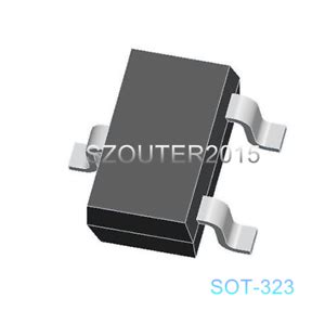
The MMBT3904 is a general-purpose NPN transistor packaged in a small SOT-23 surface-mount device (SMD) package. It is a member of the BJT family and is designed for low-power, high-speed switching applications. The transistor’s compact size and excellent performance make it a popular choice for a wide range of electronic circuits, from digital logic to analog signal conditioning.
Key Features of the MMBT3904
- NPN bipolar junction transistor
- SOT-23 surface-mount package
- High current gain (hFE)
- Fast switching speeds
- Low collector-emitter saturation voltage
- Wide operating temperature range
MMBT3904 Transistor Specifications
To effectively utilize the MMBT3904 transistor in your designs, it is essential to understand its electrical characteristics and maximum ratings. The following table summarizes the key specifications of the MMBT3904:
| Parameter | Symbol | Value | Unit |
|---|---|---|---|
| Collector-Emitter Voltage | VCEO | 40 | V |
| Collector-Base Voltage | VCBO | 60 | V |
| Emitter-Base Voltage | VEBO | 6 | V |
| Collector Current (Continuous) | IC | 200 | mA |
| Collector Current (Peak) | ICM | 500 | mA |
| Total Power Dissipation | PD | 350 | mW |
| Operating Temperature Range | TJ | -55 to 150 | °C |
| DC Current Gain (hFE) (IC = 10 mA, VCE = 1 V) | hFE | 100 to 300 | |
| Collector-Emitter Saturation Voltage (IC = 10 mA, IB = 1 mA) | VCE(sat) | 0.3 | V |
| Transition Frequency (IC = 10 mA, VCE = 20 V) | fT | 300 | MHz |
These specifications provide a foundation for understanding the capabilities and limitations of the MMBT3904 transistor. It is crucial to operate the device within these specified limits to ensure reliable performance and prevent damage to the transistor.
MMBT3904 Pinout and Package Information
The MMBT3904 transistor comes in a SOT-23 surface-mount package, which offers a compact footprint for space-constrained designs. The package has three pins: collector (C), base (B), and emitter (E). The following diagram illustrates the pinout of the MMBT3904:
When incorporating the MMBT3904 into your PCB design, ensure proper pad sizing and spacing for reliable soldering and mechanical stability. Consult the manufacturer’s datasheet for the recommended PCB land pattern and soldering guidelines.

Biasing the MMBT3904 Transistor
Proper biasing is essential for the MMBT3904 transistor to operate in the desired region and achieve the intended functionality in your circuit. The biasing condition determines whether the transistor is in the active, saturation, or cut-off region.
Common-Emitter Configuration
One of the most common biasing configurations for the MMBT3904 is the common-emitter configuration. In this configuration, the emitter is connected to ground, while the base and collector are biased with appropriate resistors. The following schematic shows a typical common-emitter biasing circuit:
The base resistor (Rb) and the collector resistor (Rc) determine the operating point of the transistor. The emitter resistor (Re) provides emitter degeneration, which improves temperature stability and linearity.
To calculate the suitable values for these resistors, you need to consider the desired collector current (Ic), the DC current gain (hFE), and the supply voltage (Vcc). The following equations can help you determine the resistor values:
Where:
– Vce is the collector-emitter voltage
– Vbe is the base-emitter voltage (typically around 0.7 V for silicon transistors)
– Ie is the emitter current (approximately equal to Ic for high hFE)
By selecting appropriate resistor values, you can ensure that the MMBT3904 operates in the desired region and provides the required performance for your specific application.

MMBT3904 Transistor Applications
The MMBT3904 transistor finds applications in a wide range of electronic circuits due to its versatility and excellent switching characteristics. Some common applications include:
- Digital Logic Circuits:
The MMBT3904 can be used as a switch in digital logic circuits, such as gates, flip-flops, and multiplexers. Its fast switching speed and low saturation voltage make it suitable for implementing high-speed digital logic. - Amplification Stages:
The MMBT3904 can be employed in small-signal amplification stages, such as pre-amplifiers, buffer amplifiers, and voltage amplifiers. Its high current gain and bandwidth enable efficient amplification of low-level signals. - Switching Circuits:
The transistor’s fast switching capabilities make it ideal for use in various switching circuits, including power switches, relay drivers, and PWM (Pulse Width Modulation) controllers. - Interfacing and Level Shifting:
The MMBT3904 can be utilized for interfacing between different voltage levels or logic families. It can act as a level shifter, allowing communication between circuits operating at different voltages. - Current Limiting and Protection:
The MMBT3904 can be employed in current limiting circuits to protect sensitive components from overcurrent conditions. It can also be used in voltage clamping and overvoltage protection circuits. - Sensor Conditioning:
In sensor applications, the MMBT3904 can be used to amplify and condition sensor outputs, such as those from temperature sensors, light sensors, or pressure sensors. - Oscillators and Timing Circuits:
The MMBT3904 can be incorporated into oscillator circuits, such as relaxation oscillators or crystal oscillators, to generate precise timing signals or clock pulses.
These are just a few examples of the many applications where the MMBT3904 transistor can be utilized. Its versatility, reliability, and performance make it a go-to choice for a wide range of electronic designs.
Practical Considerations and Tips
When using the MMBT3904 transistor in your circuits, consider the following practical tips and guidelines to ensure optimal performance and reliability:
- Heat Dissipation:
Although the MMBT3904 is rated for a maximum power dissipation of 350 mW, it is important to consider the thermal limitations of the SOT-23 package. Ensure adequate heat dissipation by providing sufficient copper area on the PCB, using thermal vias, or employing heatsinks when necessary. - Soldering Precautions:
Due to the small size of the SOT-23 package, proper soldering techniques are crucial. Use a fine-tipped soldering iron, apply an appropriate amount of solder, and avoid excessive heat exposure to prevent damage to the transistor. - Bias Resistor Selection:
When selecting bias resistors for the MMBT3904, consider the trade-offs between gain, linearity, and power consumption. Higher resistor values provide better linearity but may limit the available output current. Lower resistor values improve output drive capability but increase power dissipation. - Emitter Degeneration:
Including an emitter resistor (Re) in the biasing circuit helps to stabilize the operating point and improve temperature stability. It also enhances the linearity of the transistor’s response, reducing distortion in amplifier applications. - Noise Considerations:
In sensitive analog circuits, pay attention to the noise performance of the MMBT3904. Proper PCB layout, shielding, and filtering techniques can help minimize noise pickup and ensure a clean signal path. - Paralleling Transistors:
If higher current handling capability is required, multiple MMBT3904 transistors can be connected in parallel. However, ensure proper current sharing by using balancing resistors or matched transistors to prevent uneven current distribution. - Protection Diodes:
In inductive load switching applications, such as relay drivers, include protection diodes across the load to suppress voltage spikes and protect the transistor from reverse emitter-base breakdown.
By considering these practical aspects and following good design practices, you can harness the full potential of the MMBT3904 transistor and achieve robust and reliable performance in your electronic circuits.
Frequently Asked Questions (FAQ)
- What is the maximum collector-emitter voltage rating of the MMBT3904 transistor?
- The maximum collector-emitter voltage rating of the MMBT3904 is 40 V.
- How much continuous collector current can the MMBT3904 handle?
- The MMBT3904 can handle a continuous collector current of up to 200 mA.
- What is the typical DC current gain (hFE) of the MMBT3904?
- The typical DC current gain (hFE) of the MMBT3904 ranges from 100 to 300, measured at a collector current of 10 mA and a collector-emitter voltage of 1 V.
- Is the MMBT3904 suitable for high-frequency applications?
- Yes, the MMBT3904 has a transition frequency (fT) of 300 MHz, making it suitable for high-frequency applications within its rated operating conditions.
- Can the MMBT3904 be used as a switch in digital logic circuits?
- Yes, the MMBT3904 can be used as a switch in digital logic circuits due to its fast switching speed and low saturation voltage. It is commonly employed in various digital logic gates, flip-flops, and multiplexers.
Conclusion
The MMBT3904 NPN switching transistor is a versatile and widely used component in electronic circuits. Its high current gain, fast switching speed, and low saturation voltage make it an excellent choice for a wide range of applications, including digital logic, amplification, switching, and signal conditioning.
By understanding the MMBT3904’s specifications, biasing requirements, and practical considerations, designers can effectively incorporate this transistor into their circuits and achieve optimal performance. Whether you are working on a small-signal analog circuit or a high-speed digital system, the MMBT3904 transistor offers reliability and flexibility to meet your design needs.
As with any electronic component, proper handling, soldering, and design practices are essential to ensure the longevity and reliability of the MMBT3904 in your applications. By following the guidelines and tips provided in this article, you can confidently utilize the MMBT3904 transistor and unlock its full potential in your electronic projects.

No responses yet