Introduction to IMS PCB and the Vlak Ambient Light
Insulated Metal Substrate (IMS) printed circuit boards (PCBs) have gained significant popularity in recent years due to their excellent thermal management properties. These PCBs are particularly useful in applications that require efficient heat dissipation, such as high-power LED lighting systems. One such application is the “Vlak” ambient light, which utilizes an IMS pool PCB as its foundation.
In this article, we will explore the concept of IMS PCBs, their advantages over traditional PCBs, and how they are used in the construction of the Vlak ambient light. We will also discuss the various components that make up the IMS pool PCB and how they contribute to the overall performance of the lighting system.
What is an IMS PCB?
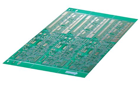
An Insulated Metal Substrate (IMS) PCB is a type of printed circuit board that consists of a metal base layer, typically aluminum, with a thin layer of dielectric material bonded to its surface. The dielectric layer is then covered with a copper foil, which is etched to create the desired circuit pattern. This unique construction allows IMS PCBs to efficiently transfer heat from the electronic components to the metal substrate, which acts as a heat sink.
Advantages of IMS PCBs over Traditional PCBs
IMS PCBs offer several advantages over traditional FR-4 PCBs:
- Superior thermal management: The metal substrate in IMS PCBs provides a direct path for heat dissipation, allowing for more efficient cooling of electronic components.
- Increased power density: Due to their excellent thermal management properties, IMS PCBs can support higher power densities than traditional PCBs.
- Improved reliability: By effectively managing heat, IMS PCBs can help extend the lifespan of electronic components and improve overall system reliability.
- Reduced size and weight: IMS PCBs can be made thinner and lighter than traditional PCBs, making them ideal for applications where space and weight are critical factors.
The Vlak Ambient Light
The Vlak ambient light is a high-performance lighting solution that utilizes an IMS pool PCB as its core component. This innovative design allows for efficient heat dissipation and uniform light distribution, creating a visually appealing and functional lighting experience.
Key Features of the Vlak Ambient Light
- Energy-efficient LED technology
- Uniform light distribution
- Dimmable functionality
- Sleek, modern design
- Easy installation and maintenance
Components of the IMS Pool PCB in the Vlak Ambient Light
The IMS pool PCB in the Vlak ambient light consists of several key components that work together to ensure optimal performance:
-
Aluminum substrate: The aluminum substrate serves as the base layer of the PCB and acts as a heat sink, efficiently transferring heat away from the electronic components.
-
Dielectric layer: A thin layer of dielectric material, typically a polymer or ceramic, is bonded to the aluminum substrate. This layer electrically insulates the copper traces from the metal substrate while allowing for efficient heat transfer.
-
Copper traces: The copper foil is etched to create the desired circuit pattern, which connects the various electronic components on the PCB.
-
LED components: High-power LEDs are mounted on the IMS PCB, with their thermal pads in direct contact with the metal substrate for optimal heat dissipation.
-
Driver circuitry: The IMS PCB also houses the driver circuitry required to power and control the LEDs, ensuring stable and efficient operation.
IMS PCB Manufacturing Process
The manufacturing process for IMS PCBs differs slightly from that of traditional PCBs due to the unique materials and construction involved. The general steps in the manufacturing process are as follows:
-
Substrate preparation: The aluminum substrate is cleaned and prepared for bonding with the dielectric layer.
-
Dielectric layer application: The dielectric material is applied to the aluminum substrate using a lamination process, ensuring a strong and uniform bond.
-
Copper foil lamination: A layer of copper foil is laminated onto the dielectric layer using heat and pressure.
-
Circuit patterning: The desired circuit pattern is transferred onto the copper foil using a photoresist and etching process.
-
Component assembly: The electronic components, including LEDs and driver circuitry, are soldered onto the IMS PCB using standard surface mount technology (SMT) techniques.
-
Testing and quality control: The assembled IMS PCB undergoes rigorous testing to ensure proper functionality and adherence to quality standards.

Thermal Management in IMS PCBs
One of the primary reasons for using IMS PCBs in the Vlak ambient light is their excellent thermal management capabilities. Understanding the principles of heat transfer and the role of the dielectric layer is essential for designing effective IMS PCBs.
Heat Transfer Mechanisms
There are three primary mechanisms of heat transfer in electronic systems:
-
Conduction: Heat transfer through direct contact between materials, such as the transfer of heat from the LED components to the aluminum substrate.
-
Convection: Heat transfer through the movement of fluids or gases, such as the transfer of heat from the aluminum substrate to the surrounding air.
-
Radiation: Heat transfer through electromagnetic waves, which is typically negligible in IMS PCBs.
Role of the Dielectric Layer
The dielectric layer in an IMS PCB plays a crucial role in both electrical insulation and thermal management. The ideal dielectric material should have the following properties:
-
High thermal conductivity: The dielectric material should allow for efficient heat transfer from the copper traces to the aluminum substrate.
-
High electrical insulation: The dielectric material should provide sufficient electrical insulation between the copper traces and the aluminum substrate to prevent short circuits and ensure proper circuit functionality.
-
Good adhesion: The dielectric material should form a strong and stable bond with both the aluminum substrate and the copper foil to ensure long-term reliability.
Common dielectric materials used in IMS PCBs include:
- Polyimide
- Epoxy
- Ceramic-filled polymers
Thermal Conductivity and Thickness of the Dielectric Layer
The thermal conductivity and thickness of the dielectric layer are critical factors in determining the overall thermal performance of an IMS PCB. A thinner dielectric layer with higher thermal conductivity will result in better heat transfer from the electronic components to the aluminum substrate.
However, there is a trade-off between thermal performance and electrical insulation. A thicker dielectric layer will provide better electrical insulation but may hinder heat transfer. It is essential to strike a balance between these two factors based on the specific requirements of the application.

IMS PCB Design Considerations for the Vlak Ambient Light
When designing the IMS pool PCB for the Vlak ambient light, several key factors must be considered to ensure optimal performance and reliability.
LED Selection and Placement
The choice of LED components and their placement on the IMS PCB are critical for achieving uniform light distribution and efficient heat dissipation. Factors to consider include:
-
LED power rating: Higher-power LEDs generate more heat, requiring more efficient thermal management.
-
LED color temperature: Different color temperatures may have different power requirements and heat generation characteristics.
-
LED spacing: Proper spacing between LEDs ensures uniform light distribution and prevents localized hot spots.
-
Thermal pad size: The size of the LED’s thermal pad should be optimized for efficient heat transfer to the aluminum substrate.
Copper Trace Design
The design of the copper traces on the IMS PCB is essential for ensuring proper electrical connectivity and minimizing power losses. Factors to consider include:
-
Trace width: Wider traces can carry more current and have lower resistance, but they also take up more space on the PCB.
-
Trace thickness: Thicker traces have lower resistance and can carry more current, but they may be more expensive to manufacture.
-
Trace routing: Proper trace routing helps minimize signal interference and ensures efficient power delivery to the LED components.
Thermal Vias
Thermal vias are plated through-holes that provide an additional path for heat transfer from the copper traces to the aluminum substrate. They are particularly useful in areas with high power density or limited surface area for heat dissipation.
When designing thermal vias, consider the following factors:
-
Via size: Larger vias can transfer more heat, but they also take up more space on the PCB.
-
Via placement: Thermal vias should be placed close to the heat-generating components for maximum effectiveness.
-
Via Fill material: The choice of via fill material, such as copper or a thermal epoxy, can impact the thermal performance of the IMS PCB.
Driver Circuitry Integration
The driver circuitry for the LED components must be integrated onto the IMS PCB in a way that ensures proper functionality and minimizes interference with the thermal management system. Factors to consider include:
-
Component selection: Choose driver components that are compatible with the LED specifications and have appropriate power ratings.
-
Component placement: Position the driver components in a way that minimizes signal interference and allows for efficient heat dissipation.
-
Grounding and shielding: Proper grounding and shielding techniques help minimize electromagnetic interference (EMI) and ensure stable operation of the driver circuitry.

Testing and Validation of the IMS Pool PCB
Once the IMS pool PCB for the Vlak ambient light has been designed and manufactured, it must undergo thorough testing and validation to ensure it meets the required performance and reliability standards.
Electrical Testing
Electrical testing verifies that the IMS PCB functions as intended and meets the specified electrical requirements. Tests may include:
-
Continuity testing: Verifying that all electrical connections are intact and there are no open circuits.
-
Insulation resistance testing: Measuring the resistance between the copper traces and the aluminum substrate to ensure proper electrical insulation.
-
Functional testing: Verifying that the LED components and driver circuitry operate as intended under various input conditions.
Thermal Testing
Thermal testing evaluates the effectiveness of the IMS PCB’s thermal management system and ensures that the LED components operate within their specified temperature ranges. Tests may include:
-
Temperature monitoring: Measuring the temperature of the LED components and the aluminum substrate under various operating conditions.
-
Thermal imaging: Using infrared cameras to identify hot spots and evaluate the uniformity of heat distribution across the IMS PCB.
-
Power cycling: Subjecting the IMS PCB to repeated power on/off cycles to assess its long-term thermal performance and reliability.
Optical Testing
Optical testing assesses the light output and distribution characteristics of the Vlak ambient light. Tests may include:
-
Luminous flux measurement: Measuring the total light output of the Vlak ambient light using an integrating sphere.
-
Luminous intensity distribution: Evaluating the uniformity of light distribution across the illuminated area using a goniophotometer.
-
Color consistency: Verifying that the color temperature and color rendering index (CRI) of the light output meet the specified requirements.
Accelerated Life Testing
Accelerated life testing subjects the IMS pool PCB to stress conditions beyond its normal operating parameters to assess its long-term reliability and identify potential failure modes. Tests may include:
-
Thermal cycling: Exposing the IMS PCB to rapid temperature changes to evaluate its resistance to thermal stress.
-
Humidity testing: Subjecting the IMS PCB to high humidity levels to assess its resistance to moisture-related failure modes.
-
Vibration testing: Exposing the IMS PCB to mechanical vibrations to evaluate its resistance to physical stress and identify potential weaknesses in component mounting or solder joints.
Future Trends and Developments in IMS PCB Technology
As the demand for high-performance, energy-efficient lighting solutions continues to grow, IMS PCB technology is expected to evolve to meet these challenges. Some of the future trends and developments in IMS PCB technology include:
-
Advanced dielectric materials: Researchers are developing new dielectric materials with higher thermal conductivity and better electrical insulation properties to enhance the performance of IMS PCBs.
-
Embedded components: Integrating passive components, such as resistors and capacitors, directly into the IMS PCB can help reduce the overall size and improve the thermal performance of the system.
-
Multi-layer IMS PCBs: Developing multi-layer IMS PCBs with additional copper layers can increase the circuit density and allow for more complex circuit designs.
-
Flexible IMS PCBs: Flexible IMS PCBs can be used in applications where conformability and flexibility are required, such as in curved or irregularly shaped lighting fixtures.
-
Smart lighting integration: Incorporating sensors, wireless connectivity, and control circuitry into IMS PCBs can enable the development of smart lighting systems that can adapt to changing environmental conditions and user preferences.
FAQ
-
What is the primary advantage of using an IMS PCB in the Vlak ambient light?
The primary advantage of using an IMS PCB in the Vlak ambient light is its excellent thermal management capabilities, which allow for efficient heat dissipation from the LED components, ensuring optimal performance and long-term reliability. -
How does the dielectric layer in an IMS PCB affect its thermal performance?
The dielectric layer in an IMS PCB acts as an electrical insulator between the copper traces and the aluminum substrate while allowing for efficient heat transfer. The thickness and thermal conductivity of the dielectric layer play a crucial role in determining the overall thermal performance of the IMS PCB. -
What are some key design considerations when developing an IMS PCB for the Vlak ambient light?
Key design considerations for an IMS PCB in the Vlak ambient light include LED selection and placement, copper trace design, thermal via incorporation, and driver circuitry integration. Each of these factors must be carefully optimized to ensure optimal performance and reliability. -
What types of testing are performed on the IMS pool PCB to ensure its quality and reliability?
The IMS pool PCB undergoes various types of testing, including electrical testing to verify functionality and insulation, thermal testing to evaluate heat management, optical testing to assess light output and distribution, and accelerated life testing to determine long-term reliability under stress conditions. -
How is IMS PCB technology expected to evolve in the future to meet the growing demands of high-performance lighting applications?
IMS PCB technology is expected to evolve through the development of advanced dielectric materials, embedded components, multi-layer designs, flexible substrates, and integration with smart lighting technologies. These advancements will enable the creation of more efficient, compact, and adaptable lighting solutions.
In conclusion, the IMS pool PCB forms the foundation of the Vlak ambient light, providing a high-performance, energy-efficient lighting solution. By leveraging the unique thermal management properties of IMS PCBs and carefully optimizing the design for LED placement, copper trace layout, and driver circuitry integration, the Vlak ambient light delivers uniform, visually appealing illumination while ensuring long-term reliability. As IMS PCB technology continues to advance, we can expect to see even more innovative and adaptable lighting solutions in the future.
No responses yet