Introduction
High Density Interconnect (HDI) Printed Circuit Boards (PCBs) have become increasingly popular in the electronics industry due to their ability to accommodate complex designs and high component density in a compact form factor. HDI PCBs utilize advanced technologies such as microvias, blind and buried vias, and fine pitch traces to achieve this high level of interconnectivity.
When it comes to designing an HDI PCB, choosing the right stackup is crucial. The stackup refers to the arrangement of copper layers, insulating layers, and vias within the PCB. The choice of stackup can significantly impact the performance, reliability, and manufacturability of the HDI PCB.
In this article, we will explore the different types of HDI PCB Stackups and discuss which stackup type is most suitable for YRAYPCB, a leading PCB manufacturer. We will also delve into the advantages and considerations of each stackup type to help you make an informed decision for your HDI PCB project.
What is an HDI PCB Stackup?
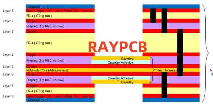
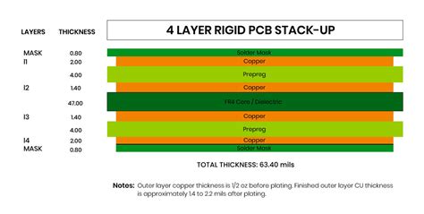
An HDI PCB stackup refers to the arrangement and configuration of the various layers that make up an HDI PCB. It defines the number of copper layers, the thickness of each layer, the type and position of vias, and the insulating materials used between the layers.
The stackup plays a vital role in determining the electrical characteristics, signal integrity, and thermal management of the HDI PCB. It also affects the manufacturing process, as different stackup types may require specific fabrication techniques and materials.
Common HDI PCB Stackup Types
There are several common HDI PCB stackup types, each with its own advantages and considerations. Let’s take a closer look at some of the most widely used stackup types:
1. 1+N+1 Stackup
The 1+N+1 stackup is a basic HDI PCB stackup that consists of two outer layers (top and bottom) and N inner layers. The outer layers are typically used for component placement and routing, while the inner layers are used for power and ground planes, as well as additional routing if needed.
| Layer | Description |
|---|---|
| Top | Component placement and routing |
| Inner | Power and ground planes, additional routing |
| Bottom | Component placement and routing |
Advantages of the 1+N+1 stackup:
– Simple and cost-effective
– Suitable for less complex designs
– Easier to manufacture compared to more advanced stackups
Considerations for the 1+N+1 stackup:
– Limited routing density and layer count
– May not be suitable for high-speed or high-frequency applications
– Limited options for via placement and routing
2. 2+N+2 Stackup
The 2+N+2 stackup is an enhanced version of the 1+N+1 stackup, with an additional outer layer on both the top and bottom sides. This stackup provides more flexibility in terms of component placement, routing, and via utilization.
| Layer | Description |
|---|---|
| Top 1 | Component placement and routing |
| Top 2 | Microvias and routing |
| Inner | Power and ground planes, additional routing |
| Bottom 2 | Microvias and routing |
| Bottom 1 | Component placement and routing |
Advantages of the 2+N+2 stackup:
– Increased routing density and layer count
– Allows for the use of microvias for higher interconnect density
– Improved signal integrity and reduced crosstalk
– Suitable for more complex designs and high-speed applications
Considerations for the 2+N+2 stackup:
– Higher manufacturing cost compared to simpler stackups
– Requires advanced fabrication techniques and materials
– May have a longer lead time due to the increased complexity
3. 3+N+3 Stackup
The 3+N+3 stackup further expands upon the 2+N+2 stackup by adding another outer layer on both the top and bottom sides. This stackup offers the highest level of design flexibility and interconnect density among the common HDI PCB stackups.
| Layer | Description |
|---|---|
| Top 1 | Component placement and routing |
| Top 2 | Microvias and routing |
| Top 3 | Microvias and routing |
| Inner | Power and ground planes, additional routing |
| Bottom 3 | Microvias and routing |
| Bottom 2 | Microvias and routing |
| Bottom 1 | Component placement and routing |
Advantages of the 3+N+3 stackup:
– Maximum routing density and layer count
– Enables the use of multiple microvia layers for highly complex designs
– Excellent signal integrity and reduced crosstalk
– Ideal for high-speed, high-frequency, and high-density applications
Considerations for the 3+N+3 stackup:
– Highest manufacturing cost among common HDI PCB stackups
– Requires advanced fabrication techniques and materials
– Longer lead time due to the increased complexity
– May require specialized design and layout expertise

Which HDI PCB Stackup Type is Right for YRAYPCB?
When choosing the right HDI PCB stackup type for your project, it’s essential to consider factors such as design complexity, performance requirements, cost, and manufacturing capabilities. At YRAYPCB, we have extensive experience in fabricating HDI PCBs with various stackup types to meet the diverse needs of our customers.
For less complex designs and cost-sensitive projects, the 1+N+1 stackup may be the most suitable option. This stackup provides a balance between simplicity and functionality, making it a popular choice for many applications.
If your design requires higher routing density, improved signal integrity, and the use of microvias, the 2+N+2 stackup is an excellent choice. This stackup offers increased flexibility and performance compared to the 1+N+1 stackup, while still maintaining a reasonable manufacturing cost.
For the most demanding applications that require the highest level of interconnect density, signal integrity, and performance, the 3+N+3 stackup is the way to go. This stackup provides the maximum routing density and enables the use of multiple microvia layers, making it ideal for complex, high-speed, and high-frequency designs.
At YRAYPCB, we work closely with our customers to understand their specific requirements and help them select the most appropriate HDI PCB stackup type for their project. Our team of experienced engineers and PCB designers can provide guidance and support throughout the design and manufacturing process to ensure the best possible outcome.

Frequently Asked Questions (FAQ)
- What is the difference between an HDI PCB and a standard PCB?
- HDI PCBs utilize advanced technologies such as microvias, blind and buried vias, and fine pitch traces to achieve higher interconnect density and improved performance compared to standard PCBs.
- How do I choose the right HDI PCB stackup type for my project?
- When choosing the right HDI PCB stackup type, consider factors such as design complexity, performance requirements, cost, and manufacturing capabilities. Consult with your PCB manufacturer to determine the most suitable stackup type for your specific needs.
- What are the advantages of using a 3+N+3 stackup for HDI PCBs?
- The 3+N+3 stackup offers the highest level of design flexibility, interconnect density, and performance among common HDI PCB stackups. It enables the use of multiple microvia layers, provides excellent signal integrity, and is ideal for high-speed, high-frequency, and high-density applications.
- How does the choice of HDI PCB stackup affect the manufacturing cost?
- Generally, more advanced HDI PCB stackups, such as 2+N+2 and 3+N+3, have higher manufacturing costs compared to simpler stackups like 1+N+1. This is due to the increased complexity, use of advanced fabrication techniques, and specialized materials required for these stackups.
- Can YRAYPCB help me select the right HDI PCB stackup for my project?
- Yes, at YRAYPCB, we have a team of experienced engineers and PCB designers who can work closely with you to understand your specific requirements and help you select the most appropriate HDI PCB stackup type for your project. We provide guidance and support throughout the design and manufacturing process to ensure the best possible outcome.

Conclusion
Choosing the right HDI PCB stackup type is crucial for the success of your electronics project. Each stackup type has its own advantages and considerations, and the selection process should take into account factors such as design complexity, performance requirements, cost, and manufacturing capabilities.
At YRAYPCB, we have the expertise and experience to help you navigate the complexities of HDI PCB design and manufacturing. Whether you need a simple 1+N+1 stackup for a cost-sensitive project or a highly advanced 3+N+3 stackup for a cutting-edge application, we have the solutions to meet your needs.
By partnering with YRAYPCB for your HDI PCB project, you can benefit from our state-of-the-art manufacturing facilities, skilled engineers, and commitment to quality. We strive to deliver the best possible results for our customers, ensuring that your HDI PCBs meet the highest standards of performance, reliability, and manufacturability.
Don’t hesitate to reach out to us for more information on HDI PCB stackups and how we can help bring your electronics project to life. Trust YRAYPCB to be your reliable partner in HDI PCB design and manufacturing.

No responses yet