Introduction to Fly Buck Converters and PCB layout
Fly buck converters, also known as synchronous buck converters, are highly efficient DC-DC converters used to step down voltage levels in various electronic applications. Proper PCB layout is crucial for achieving optimal performance, minimizing noise, and ensuring the reliability of the converter. In this article, we will discuss essential tips and guidelines for designing a fly buck converter PCB layout.
Understanding the Basics of Fly Buck Converters
A fly buck converter consists of several key components, including:
- Input capacitor
- High-side and low-side MOSFETs
- Inductor
- Output capacitor
- Control IC
The converter works by rapidly switching the MOSFETs on and off, allowing current to flow through the inductor and charge the output capacitor. This process effectively steps down the input voltage to the desired output voltage level.

Key Considerations for Fly Buck Converter PCB Layout
When designing a PCB layout for a fly buck converter, several factors must be taken into account to ensure optimal performance:
- Component placement
- Trace routing
- Grounding
- Thermal management
- EMI reduction
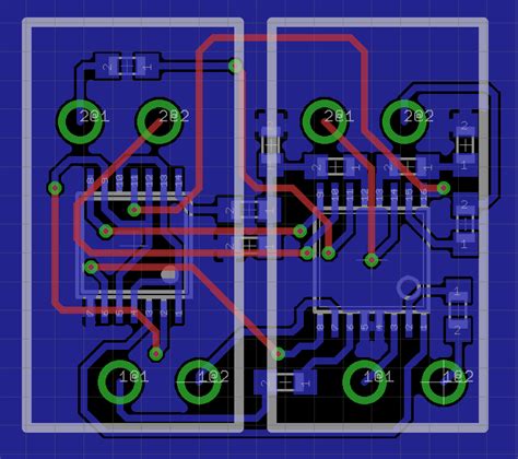
Component Placement
Proper component placement is essential for minimizing trace lengths, reducing parasitic inductance, and improving overall efficiency. Follow these guidelines for optimal component placement:
- Place the input capacitor as close to the MOSFETs as possible to minimize the input loop area.
- Position the high-side and low-side MOSFETs close together to reduce the switching loop area.
- Keep the inductor close to the MOSFETs to minimize trace lengths and reduce resistive losses.
- Place the output capacitor near the load to minimize output voltage ripple.
- Locate the control IC away from the power components to avoid noise coupling.
Trace Routing
Proper trace routing is critical for reducing resistive losses, minimizing inductance, and improving overall efficiency. Consider the following tips when routing traces:
- Use wide traces for high-current paths to minimize resistive losses.
- Keep the high-current loops (input loop and switching loop) as small as possible to reduce inductance.
- Avoid sharp corners and use 45-degree angles when routing traces to reduce EMI.
- Use a ground plane to provide a low-impedance return path for currents.
- Route the feedback trace away from the power components to avoid noise coupling.
Grounding
A solid grounding scheme is essential for minimizing noise, reducing ground loops, and improving overall performance. Follow these grounding guidelines:
- Use a single-point ground (star ground) for the power components to avoid ground loops.
- Connect the ground planes of the power and control sections using a single, low-impedance path.
- Provide separate ground planes for analog and digital components to reduce noise coupling.
- Use vias to connect the ground planes on different layers of the PCB.
Thermal Management
Effective thermal management is necessary to prevent overheating and ensure the long-term reliability of the fly buck converter. Consider these thermal management techniques:
- Use a large ground plane to dissipate heat from the power components.
- Provide adequate copper area for the MOSFETs and inductor to enhance heat dissipation.
- Consider using thermal vias to transfer heat from the top layer to the inner layers and bottom layer of the PCB.
- Use a heatsink or other cooling methods if necessary, depending on the power requirements of the converter.
EMI Reduction
Minimizing electromagnetic interference (EMI) is crucial for ensuring the converter’s compatibility with other electronic devices and meeting regulatory requirements. Employ these techniques to reduce EMI:
- Keep the high-current loops as small as possible to minimize the antenna effect.
- Use a ground plane to provide shielding and reduce radiated EMI.
- Implement proper filtering at the input and output of the converter using capacitors and ferrite beads.
- Consider using a shielded inductor or a toroidal inductor to minimize radiated EMI.
- Follow proper layout techniques, such as avoiding sharp corners and using 45-degree angles when routing traces.

PCB Layer Stackup for Fly Buck Converters
A well-designed PCB layer stackup is essential for achieving optimal performance and minimizing noise in a fly buck converter. A typical 4-layer stackup for a fly buck converter PCB is as follows:
| Layer | Purpose |
|---|---|
| Top | Power components, input/output capacitors, control IC |
| Inner1 | Ground plane |
| Inner2 | Power plane (input voltage) |
| Bottom | Signal traces, feedback trace, additional components |
This stackup provides a solid ground plane for current return paths, a power plane for distributing the input voltage, and separate layers for power components and signal traces to minimize noise coupling.

Component Selection for Fly Buck Converters
Choosing the right components is crucial for achieving optimal performance and reliability in a fly buck converter. Consider these factors when selecting components:
- MOSFETs: Select MOSFETs with low on-resistance (RDS(on)) and low gate charge (Qg) to minimize conduction and switching losses.
- Inductor: Choose an inductor with low DC resistance (DCR) and high saturation current rating to minimize resistive losses and prevent saturation.
- Capacitors: Use low-ESR (equivalent series resistance) capacitors for the input and output to minimize voltage ripple and improve efficiency.
- Control IC: Select a control IC that offers the required features, such as adjustable switching frequency, soft-start, and protection functions.
Testing and Debugging Fly Buck Converter PCBs
After the PCB layout is complete and the components are assembled, it is essential to test and debug the fly buck converter to ensure proper operation and identify any issues. Follow these steps for testing and debugging:
- Visual inspection: Inspect the PCB for any manufacturing defects, such as solder bridges, Cold Solder Joints, or damaged components.
- Continuity test: Use a multimeter to check for continuity between various points on the PCB, ensuring that there are no short circuits or open connections.
- Power-on test: Apply the input voltage to the converter and measure the output voltage to verify that it meets the desired specifications.
- Efficiency measurement: Measure the input and output power of the converter to calculate its efficiency and compare it with the expected values.
- Ripple measurement: Use an oscilloscope to measure the output voltage ripple and ensure that it is within acceptable limits.
- Thermal monitoring: Monitor the temperature of the power components using a thermal camera or temperature sensors to ensure that they are operating within their safe limits.
Troubleshooting Common Issues in Fly Buck Converter PCBs
If the fly buck converter PCB does not perform as expected, consider these common issues and their solutions:
- Output voltage is too low:
- Check the input voltage and ensure that it is within the specified range.
- Verify that the inductor value is correct and that it is not saturated.
-
Check the MOSFET gate drive signals and ensure that they are properly switching.
-
Output voltage ripple is too high:
- Increase the output capacitance or use capacitors with lower ESR.
- Reduce the inductor ripple current by increasing the inductance value or the switching frequency.
-
Check the PCB layout and ensure that the output capacitor is placed close to the load.
-
Converter is overheating:
- Verify that the MOSFETs and inductor are properly sized for the current requirements.
- Check the PCB layout and ensure that there is adequate copper area for heat dissipation.
-
Consider using a heatsink or other cooling methods if necessary.
-
Converter is unstable or oscillating:
- Check the feedback loop compensation and ensure that it is properly designed.
- Verify that the PCB layout follows the guidelines for minimizing noise and promoting stability.
- Ensure that the input and output capacitors are properly sized and have low ESR.
Best Practices for Fly Buck Converter PCB Layout
To summarize, follow these best practices when designing a fly buck converter PCB layout:
- Place components strategically to minimize trace lengths and loop areas.
- Use wide traces for high-current paths and keep the high-current loops small.
- Implement a solid grounding scheme using a single-point ground and separate ground planes for power and control sections.
- Provide adequate copper area for heat dissipation and consider using thermal vias or heatsinks if necessary.
- Minimize EMI by keeping high-current loops small, using a ground plane for shielding, and implementing proper filtering.
- Choose a suitable PCB layer stackup with dedicated layers for power components, ground, and signal traces.
- Select components with low losses and high performance, such as low-RDS(on) MOSFETs and low-DCR inductors.
- Test and debug the PCB thoroughly, measuring key parameters such as output voltage, efficiency, and thermal performance.
Frequently Asked Questions (FAQ)
-
What is a fly buck converter, and how does it differ from a regular buck converter?
A fly buck converter, also known as a synchronous buck converter, uses two MOSFETs (high-side and low-side) instead of a single MOSFET and a diode used in a regular buck converter. This configuration allows for higher efficiency and lower power losses, especially at low output voltages. -
Why is PCB layout important for fly buck converters?
PCB layout is crucial for fly buck converters because it directly impacts the converter’s performance, efficiency, and reliability. A well-designed layout minimizes trace lengths, reduces loop areas, and promotes proper grounding and thermal management, all of which contribute to optimal converter operation. -
What are the key components of a fly buck converter?
The key components of a fly buck converter include the input capacitor, high-side and low-side MOSFETs, inductor, output capacitor, and control IC. Each component plays a critical role in the converter’s operation and must be carefully selected and placed on the PCB. -
How can I reduce EMI in my fly buck converter PCB layout?
To reduce EMI in a fly buck converter PCB layout, minimize the high-current loop areas, use a ground plane for shielding, implement proper filtering at the input and output, and follow layout techniques such as avoiding sharp corners and using 45-degree angles when routing traces. Additionally, consider using shielded or toroidal inductors to minimize radiated EMI. -
What should I do if my fly buck converter PCB is not performing as expected?
If your fly buck converter PCB is not performing as expected, first conduct a thorough visual inspection and continuity test to identify any manufacturing defects or assembly issues. Then, measure key parameters such as output voltage, efficiency, and ripple, and compare them with the expected values. If issues persist, review the PCB layout, component selection, and feedback loop compensation, and make necessary adjustments to improve performance.
By following these tips and guidelines, you can design a fly buck converter PCB layout that achieves optimal performance, efficiency, and reliability. Remember to carefully consider component placement, trace routing, grounding, thermal management, and EMI reduction, and always test and debug your PCB thoroughly to ensure proper operation.
No responses yet